ADC120
Datasheet
8-channel, 50 ksps to 1 Msps, 12-bit A/D converter
Features
•
•
•
•
•
•
•
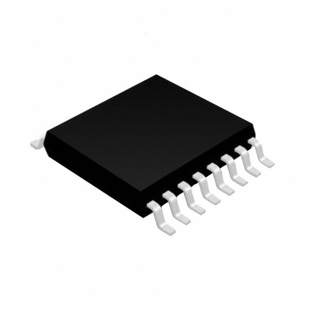
TSSOP-16
50 ksps to 1 Msps conversion rate
8-to-1-channel input MUX
3.3 V operating supply
Pure CMOS
Very low consumption
SPI, serial digital output
Power-down function
Applications
•
•
•
Shunt resistor detector
Analog multiplexing and conversion
Telemetry
Description
The ADC120 is a low-power, eight-channel pure CMOS 12-bit analog-to-digital
converter specified for conversion from 50 ksps to 1 Msps, tested at 1 Msps. The
architecture is based on a successive-approximation register with an internal trackand-hold cell. The ADC120 features 8 single ended multiplexed inputs. The output
serial data is straight binary and is SPI™ compatible.
Maturity status link
ADC120
The analog and digital power supplies operate from 2.7 V to 3.6 V. The power
consumption at 3.3 V nominal supply is as low as 6.6 mW. The ADC120 comes
plastic TSSOP-16, and can operates from -40 °C to +125 °C ambient temperature.
Device summary
Order code
ADC120IPT
Temperature
range
-40 °C to +125 °C
Package
TSSOP-16
Marking
ADC120I
DS12987 - Rev 1 - April 2019
For further information contact your local STMicroelectronics sales office.
www.st.com
�ADC120
Functional description
1
Functional description
Figure 1. Pin description (top view)
/CS
1
16
SCLK
AVCC
2
15
DOUT
AGND
3
14
DIN
IN0
4
13
DVCC
IN1
5
12
DGND
IN2
6
11
IN7
IN3
7
10
IN6
IN4
8
9
IN5
Figure 2. Block diagram
IN0
Input
Mux.
AVCC
12 bit
SAR
ADC
T/H
IN7
AGND
AGND
DVCC
/CS
SCLK
DIN
DOUT
DGND
Control
Logic
Table 1. Control register bits
Bit#
7 (MSB)
Symbol
6
Any code except 11
5
4
3
ADD2
ADD1
ADD0
2
1
0
Any code except 001
Table 2. Control register bit description
DS12987 - Rev 1
Bit#
Symbol
Description
7, 6, 2, 1, 0
DONTC
Don’t care (forbidden codes provided in Table 1. Control register bits)
5
ADD2
4
ADD1
3
ADD0
They determine which input channel converted, as per Table 3. Input channel
description.
page 2/15
�ADC120
Functional description
Table 3. Input channel description
DS12987 - Rev 1
ADD2
ADD1
ADD0
Input channel
0
0
0
IN0
0
0
1
IN1
0
1
0
IN2
0
1
1
IN3
1
0
0
IN4
1
0
1
IN5
1
1
0
IN6
1
1
1
IN7
page 3/15
�ADC120
Maximum ratings and operating conditions
2
Maximum ratings and operating conditions
Absolute maximum ratings are those values beyond which damage to the device may occur. Functional operation
under these conditions is not implied.
Table 4. Absolute maximum ratings
Symbol
Parameters
Value
Units
AVCC (1)
Maximum analog power supply between AVCC and
AGND
-0.3 V to 4.8 V
V
DVCC (1)
Maximum digital power supply between DVCC and
DGND
-0.3 V to AVCC +0.3 V (max 4.8 V)
V
Tstg
Maximum temperature storage
-65 to +150
°C
Tj
Maximum junction temperature
+150
°C
Rthja (2)
Junction to ambient thermal resistance (TSSOP16
package)
95
°C/W
Rthjc (2)
Junction to case thermal resistance (TSSOP16
package)
35
°C/W
-0.3 V to AVCC +0.3 V
V
Max input current at any pin
± 10
mA
HBM on all pins (human body model)
±4k
V
CDM on all pins (charged device model)
±1k
V
Vi (3)
Ii
ESD
Max voltage on any pin vs. GND
1. All voltages, except differential I/O bus voltage, are with respect to the network ground terminal.
2. Short-circuits can cause excessive heating. Destructive dissipation can result from short-circuits on the amplifiers.
3. When the input voltage at any pin exceeds the power supplies (that is VIN < AGND or VIN > AVCC or DVCC), the current at
that pin should be limited to 10 mA. The 20 mA maximum package input current rating limits the number of pins that can
safely exceed the power supplies with an input current of 10 mA to two.
Table 5. Operating conditions
Symbol
Min.
Max.
Units
AVCC
Analog supply voltage
2.7
3.6
V
DVCC
Digital supply voltage
AVCC - 0.15 V
AVCC + 0.15 V
V
VINA
Analog input voltage
0
AVCC
V
VIND
Digital input voltage
0
AVCC
V
SCLK
Clock frequency
0.8
16
MHz
Ambient temperature range
-40
+125
°C
Ta
DS12987 - Rev 1
Parameters
page 4/15
�ADC120
Electrical characteristics
3
Electrical characteristics
AVCC = DVCC = + 3.3 V, Single-ended input, AGND = DGND = 0 V, fSCLK = 16 MHz, fSAMPLE = 1 Msps,
CL = 25 pF, Ta = 25 °C, unless otherwise specified.
Table 6. Electrical characteristics
Symbol
Parameters
Test conditions
Min.
Typ.
Max
Unit
12
Bits
Static characteristics
Resolution with no missing
codes
INL
Integral non-linearity (end
point method)
-1.1
±0.4
1.1
LSB
DNL
Differential non-linearity
-0.8
±0.4
0.8
LSB
OE
Offset error
-2.3
0.8
2.3
LSB
2.3
LSB
OEM
Offset error match
FSE
Full scale error
FSEM
0.8
-2.3
Full scale error match
0.8
0.8
LSB
68.9
72
dB
71
73
dB
Dynamic characteristics
SINAD
SNR
THD
Signal-to-noise plus
distortion ratio (0 to Fs/2)
Signal-to-noise ratio
(0 to Fs/2)
Total harmonic distortion
FIN = 40.2 kHz, −0.02 dBFS
−80
SFDR
Spurious-free dynamic
range (0 to Fs/2)
74
ENOB
Effective number of bits
11.1
ISO
Channel-to-channel isolation FIN = 20 kHz, −0.02 dBFS
IM2
2nd order intermodulation
IM3
3dr order intermodulation
fa = 19.5 kHz, fb = 20.5 kHz
VINA = VINB = -6.02 dBFS
fa = 19.5 kHz, fb = 20.5 kHz
VINA = VINB = -6.02 dBFS
-73
dB
dB
11.7
Bits
84
dB
−90
dB
−90
dB
Analog input characteristics
IDCL
DC leakage current
CINA
Input capacitance
-1
1
µA
Track mode
45
pF
Hold mode
4.5
pF
Digital input characteristics
VIH
Input high voltage
VIL
Input low voltage
IIN
Digital input current
CIND
2.1
VIN = 0 V or DVCC
V
-1
Digital input capacitance
4.5
0.8
V
1
µA
pF
Digital output characteristics (output coding: straight (natural) binary)
VOH(1)
DS12987 - Rev 1
Output high voltage
Isource = 1 mA
2.8
V
page 5/15
�ADC120
Electrical characteristics
Symbol
VOL(1)
Parameters
Output low voltage
IOZH, IOZL
Hi-impedance output
leakage current
COUT
Hi-impedance output
capacitance
Test conditions
Min.
Typ.
Isink = 1 mA
-1
Max
Unit
0.4
V
1
µA
4.5
pF
Power supply characteristic
IAVCC + IDVCC
Total supply current, normal
mode (CS low)
Total supply current,
shutdown mode (CS high)
AVCC = DVCC = +2.7 V to
+3.6 V, fS = 1 MSPS,
2
mA
5
µA
13
SCLK
cycles
60
%
3
SCLK
cycles
16
SCLK
cycles
FIN = 40 kHz
AVCC = DVCC = +2.7 V to
+3.6 V, fS = 0
AC characteristics (AVCC = DVCC = +2.7 V to +3.6 V)
tCONVERT
Conversion (Hold) time
DC
SCLK duty cycle
tACQ
Acquisition (Track) Time
cycles
40
See figure 3
Throughput time Acquisition
time + Conversion time
tAD
Aperture delay
4
ns
Timing specifications (AVCC = DVCC = +2.7 V to +3.6 V) (2)
tCSH
CS/ hold time after SCLK
rising edge
(3)
10
0
ns
tCSS
CS/ setup time prior SCLK
rising edge
(3)
10
4.5
ns
tEN
CS/falling edge to DOUT
enabled
tDACC
DOUT access time after
SCLK falling edge
tDHLD
DOUT hold time after SCLK
falling edge
7
tDS
DIN setup time prior to
SCLK rising edge
10
ns
tDH
DIN hold time after SCLK
rising edge
10
ns
tDIS
CS/ rising edge to DOUT
high-impedance
tCH
Min. SCLK high time
0.4 x tSCLK
ns
tCL
Min. SCLK low time
0.4 x tSCLK
ns
Load 25 pF
5
30
ns
17
27
ns
4
ns
DOUT falling
2.4
20
DOUT rising
0.9
20
ns
1. Limits are guaranteed by functional test.
2. Limits are guaranteed by design or characterization.
3. Clock may be in any state (high or low) when CS/ goes high. Setup and hold time restrictions apply only to CS/ going low.
DS12987 - Rev 1
page 6/15
�ADC120
Timing diagrams
4
Timing diagrams
Figure 3. Timings
DS12987 - Rev 1
page 7/15
�ADC120
Definitions
5
Definitions
Acquisition Time is the time required to acquire the input voltage. During this time, the hold capacitor is charged
by the input voltage.
Aperture Delay is the time between the fourth falling edge of SCLK and the time when the input signal is
internally acquired or held for conversion.
Channel-to-channel isolation is the residual noise injected on the selected channel by other unselected
channels.
Conversion Time is the time required, after the input voltage is acquired, to convert the input voltage to a digital
word.
Differential Non-Linearity (DNL) is the maximum deviation from the ideal step size of 1 LSB.
Duty cycle is the ratio, for a periodic digital signal, of the high level duration divided by the total period.
Effective Number of Bits (ENOB) is a method of specifying Signal-to-Noise and Distortion or SINAD. ENOB is
defined as (SINAD - 1.76) / 6.02 and says that the converter is equivalent to a perfect ADC of this (ENOB)
number of bits.
Full Power Bandwidth is a measure of the frequency at which the reconstructed output fundamental drops 3dB
below its low frequency value for a full scale input.
Full Scale Error (single-ended input) is the deviation of the last code transition (111...110) to (111...111) from the
ideal (AVCC - 1.5 LSB or -1LSB), after adjusting for offset error.
Positive Full Scale Error (differential input) is the deviation of the last code transition (111...110) to (111...111)
from the ideal (AVCC - 1.5 LSB or -1LSB), after adjusting for offset error.
Negative Full Scale Error (differential input) is the deviation of the last code transition (111...110) to (111...111)
from the ideal (-AVCC + 1.5 LSB or +1LSB), after adjusting for offset error.
Integral Non-Linearity(INL) is the deviation of each individual code from a line drawn from negative full scale (½
LSB below the first code transition) through positive full scale (½ LSB above the last code transition). The
deviation of any given code from this straight line is measured from the center of that code value.
Intermodulation distortion (IMD) is the results of the product of two pure sinewaves at frequency fa and fb
applied to the ADC input. To avoid clipping when the sinewave are in phase, the level must be just below -6dBFS.
Assuming that the level of the two tones is equal, IMD2 is the difference in dBc between level(fa or fb) and level(fa
± fb). IMD3 is is the difference in dBc between level(fa or fb) and level(2fa ± fb) or level(fa ± 2fb).
Missing Codes are those output codes that will never appear at the ADC outputs. The ADC120 is guaranteed not
to have any missing codes.
Offset Error (Single-ended input) is the deviation of the first code transition (000...000) to (000...001) from the
ideal (i.e. GND +1 LSB).
Offset Error (Differential input) is the deviation of the mid-code transition (01…111) to (10…000) from the ideal
(i.e. AVCC/2 +1 LSB).
Signal to Noise Ratio (SNR) is the ratio, expressed in dB, of the rms value of the fundamental of input signal to
the rms value of the sum of all other spectral components below one-half the sampling frequency, not including
harmonics or DC-component.
Signal to Noise Plus Distortion (S/N+D or SINAD) is the ratio of the rms value of the fundamental of input
signal to the rms value of all of the other spectral components below half the sampling frequency, including
harmonics but excluding DC-component.
Spurious Free Dynamic Range (SFDR) is the difference, expressed in dB, between the desired signal amplitude
of fundamental to the amplitude of the peak spurious spectral component, where a spurious spectral component
is any signal present in the output spectrum that is not present at the input and may or may not be a harmonic.
Total Harmonic Distortion (THD) is the ratio, expressed in dBc, of the rms total of the first nine harmonic
components at the output to the rms level of fundamental of the input signal frequency as seen at the output. THD
is calculated as THD = 20log10 [sqrt((Af2²+…+Af10²)/Af1²)]
where Af1 is the RMS power of the fundamental at the output and Af2 to Af10 are the RMS power in the first nine
harmonic frequencies.
Throughput Time is the minimum time required between the start of two successive conversions. It is the
acquisition time plus the conversion time.
DS12987 - Rev 1
page 8/15
�ADC120
Package information
6
Package information
In order to meet environmental requirements, ST offers these devices in different grades of ECOPACK packages,
depending on their level of environmental compliance. ECOPACK specifications, grade definitions and product
status are available at: www.st.com. ECOPACK is an ST trademark.
6.1
TSSOP-16 package information
Figure 4. TSSOP-16 package outline
DS12987 - Rev 1
page 9/15
�ADC120
TSSOP-16 package information
Table 7. TSSOP-16 package mechanical data
Dim.
mm
Min.
Typ.
A
1.20
A1
0.05
A2
0.80
b
0.19
0.30
c
0.09
0.20
D
4.90
5.00
5.10
E
6.20
6.40
6.60
E1
4.30
4.40
4.50
e
0°
L
0.45
aaa
0.15
1.00
1.05
0.65
k
L1
DS12987 - Rev 1
Max.
8°
0.60
0.75
1.00
0.10
page 10/15
�ADC120
Revision history
Table 8. Document revision history
DS12987 - Rev 1
Date
Version
11-Apr-2019
1
Changes
Initial release.
page 11/15
�ADC120
Contents
Contents
1
Functional description . . . . . . . . . . . . . . . . . . . . . . . . . . . . . . . . . . . . . . . . . . . . . . . . . . . . . . . . . . . . . 2
2
Maximum ratings and operating conditions . . . . . . . . . . . . . . . . . . . . . . . . . . . . . . . . . . . . . . . . 4
3
Electrical characteristics. . . . . . . . . . . . . . . . . . . . . . . . . . . . . . . . . . . . . . . . . . . . . . . . . . . . . . . . . . . 5
4
Timing diagrams. . . . . . . . . . . . . . . . . . . . . . . . . . . . . . . . . . . . . . . . . . . . . . . . . . . . . . . . . . . . . . . . . . .7
5
Definitions. . . . . . . . . . . . . . . . . . . . . . . . . . . . . . . . . . . . . . . . . . . . . . . . . . . . . . . . . . . . . . . . . . . . . . . . .8
6
Package information. . . . . . . . . . . . . . . . . . . . . . . . . . . . . . . . . . . . . . . . . . . . . . . . . . . . . . . . . . . . . . .9
6.1
TSSOP-16 package information . . . . . . . . . . . . . . . . . . . . . . . . . . . . . . . . . . . . . . . . . . . . . . . . . . 9
Revision history . . . . . . . . . . . . . . . . . . . . . . . . . . . . . . . . . . . . . . . . . . . . . . . . . . . . . . . . . . . . . . . . . . . . . . .11
Contents . . . . . . . . . . . . . . . . . . . . . . . . . . . . . . . . . . . . . . . . . . . . . . . . . . . . . . . . . . . . . . . . . . . . . . . . . . . . . .12
List of tables . . . . . . . . . . . . . . . . . . . . . . . . . . . . . . . . . . . . . . . . . . . . . . . . . . . . . . . . . . . . . . . . . . . . . . . . . .13
List of figures. . . . . . . . . . . . . . . . . . . . . . . . . . . . . . . . . . . . . . . . . . . . . . . . . . . . . . . . . . . . . . . . . . . . . . . . . .14
DS12987 - Rev 1
page 12/15
�ADC120
List of tables
List of tables
Table 1.
Table 2.
Table 3.
Table 4.
Table 5.
Table 6.
Table 7.
Table 8.
Control register bits . . . . . . . . . . . . .
Control register bit description . . . . . .
Input channel description . . . . . . . . .
Absolute maximum ratings . . . . . . . .
Operating conditions . . . . . . . . . . . .
Electrical characteristics . . . . . . . . . .
TSSOP-16 package mechanical data .
Document revision history . . . . . . . . .
DS12987 - Rev 1
.
.
.
.
.
.
.
.
.
.
.
.
.
.
.
.
.
.
.
.
.
.
.
.
.
.
.
.
.
.
.
.
.
.
.
.
.
.
.
.
.
.
.
.
.
.
.
.
.
.
.
.
.
.
.
.
.
.
.
.
.
.
.
.
.
.
.
.
.
.
.
.
.
.
.
.
.
.
.
.
.
.
.
.
.
.
.
.
.
.
.
.
.
.
.
.
.
.
.
.
.
.
.
.
.
.
.
.
.
.
.
.
.
.
.
.
.
.
.
.
.
.
.
.
.
.
.
.
.
.
.
.
.
.
.
.
.
.
.
.
.
.
.
.
.
.
.
.
.
.
.
.
.
.
.
.
.
.
.
.
.
.
.
.
.
.
.
.
.
.
.
.
.
.
.
.
.
.
.
.
.
.
.
.
.
.
.
.
.
.
.
.
.
.
.
.
.
.
.
.
.
.
.
.
.
.
.
.
.
.
.
.
.
.
.
.
.
.
.
.
.
.
.
.
.
.
.
.
.
.
.
.
.
.
.
.
.
.
.
.
.
.
.
.
.
.
.
.
.
.
.
.
.
.
.
.
.
.
.
.
.
.
.
.
.
.
.
.
.
.
.
.
.
.
.
.
.
.
.
.
.
.
.
.
.
.
.
.
.
.
.
.
.
.
.
.
.
.
.
.
.
.
.
.
.
.
.
.
.
.
.
.
.
.
.
.
.
.
.
.
.
.
.
.
.
.
.
.
.
.
.
.
.
.
.
.
.
.
.
.
.
.
.
.
.
.
.
.
.
.
.
.
.
.
.
.
.
.
.
.
.
.
.
.
.
.
.
.
.
.
.
.
.
.
.
.
.
.
.
.
.
.
.
.
.
.
.
.
.
.
.
.
.
.
.
.
.
.
.
.
.
.
.
.
.
.
.
.
.
.
.
.
.
.
.
.
. 2
. 2
. 3
. 4
. 4
. 5
10
11
page 13/15
�ADC120
List of figures
List of figures
Figure 1.
Figure 2.
Figure 3.
Figure 4.
DS12987 - Rev 1
Pin description (top view) . .
Block diagram . . . . . . . . .
Timings . . . . . . . . . . . . . .
TSSOP-16 package outline
.
.
.
.
.
.
.
.
.
.
.
.
.
.
.
.
.
.
.
.
.
.
.
.
.
.
.
.
.
.
.
.
.
.
.
.
.
.
.
.
.
.
.
.
.
.
.
.
.
.
.
.
.
.
.
.
.
.
.
.
.
.
.
.
.
.
.
.
.
.
.
.
.
.
.
.
.
.
.
.
.
.
.
.
.
.
.
.
.
.
.
.
.
.
.
.
.
.
.
.
.
.
.
.
.
.
.
.
.
.
.
.
.
.
.
.
.
.
.
.
.
.
.
.
.
.
.
.
.
.
.
.
.
.
.
.
.
.
.
.
.
.
.
.
.
.
.
.
.
.
.
.
.
.
.
.
.
.
.
.
.
.
.
.
.
.
.
.
.
.
.
.
.
.
.
.
.
.
.
.
.
.
.
.
.
.
.
.
.
.
.
.
.
.
.
.
.
.
.
.
.
.
.
.
.
.
.
.
.
.
.
.
.
.
.
.
.
.
.
.
.
.
.
.
.
.
.
.
.
.
.
.
.
.
.
.
2
2
7
9
page 14/15
�ADC120
IMPORTANT NOTICE – PLEASE READ CAREFULLY
STMicroelectronics NV and its subsidiaries (“ST”) reserve the right to make changes, corrections, enhancements, modifications, and improvements to ST
products and/or to this document at any time without notice. Purchasers should obtain the latest relevant information on ST products before placing orders. ST
products are sold pursuant to ST’s terms and conditions of sale in place at the time of order acknowledgement.
Purchasers are solely responsible for the choice, selection, and use of ST products and ST assumes no liability for application assistance or the design of
Purchasers’ products.
No license, express or implied, to any intellectual property right is granted by ST herein.
Resale of ST products with provisions different from the information set forth herein shall void any warranty granted by ST for such product.
ST and the ST logo are trademarks of ST. For additional information about ST trademarks, please refer to www.st.com/trademarks. All other product or service
names are the property of their respective owners.
Information in this document supersedes and replaces information previously supplied in any prior versions of this document.
© 2019 STMicroelectronics – All rights reserved
DS12987 - Rev 1
page 15/15
�