AEK-COM-GNSST31
Data brief
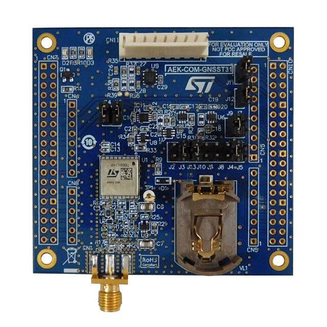
GNSS evaluation board based on Teseo-LIV3F for SPC5 microcontrollers
Features
•
•
•
•
•
•
•
•
•
•
•
•
•
Product summary
GNSS evaluation
board based on
AEK-COMGNSST31
Teseo-LIV3F for
SPC5 microcontrollers
Tiny GNSS module
Teseo-LIV3F
Code generator, quick
resource configurator
and Eclipse
SPC5-STUDIO
development
environment for SPC5
MCUs
AutoDevKit library
plugin for SPC5STUDIO
STSWAUTODEVKIT
Global navigation
satellite system
software expansion
for STM32Cube
X-CUBE-GNSS1
Sensitivity: -162 dBm indoor (tracking mode)
Interfaces:
–
UART and I²C ports
–
Configurable digital I/O timepulse
–
EXTINT input for wakeup
NMEA protocol
Assisted GNSS:
–
Predictive autonomous
–
Predictive server-based
–
Real-time server-based
Compatible with SPC5
LNA and SAW filter on the RF path
SMA female antenna connector
Battery holder
Highly compact design: 70 x 65 mm
Operating supply voltage: 3.3 - 5 V
Ambient temperature: -40/+85 °C
Part of the AutoDevKit™ initiative
RoHS and WEEE compliant
Description
The AEK-COM-GNSST31 evaluation board is based on the certified Teseo-LIV3F
global navigation satellite system (GNSS) module with embedded TeseoIII single die
standalone positioning receiver IC.
The tiny, affordable, and easy-to use module guarantees superior accuracy and
reduced time to first fix (TTFF) thanks to the on-board 26 MHz temperature
compensated crystal oscillator (TCXO) and dedicated 32 KHz real-time clock (RTC)
oscillator.
The evaluation package is used in conjunction with the X-CUBE-GNSS1 firmware to
provide the necessary acquisition, tracking, navigation and data output functionality
without external memory support.
The AEK-COM-GNSST31 evaluation board can be readily connected with an SPC5
MCU for automotive application development as part of the AutoDevKit™ initiative.
Tracking
Applications
Smart City
GNSS/GPS
Mobility Services
DB4131 - Rev 1 - February 2020
For further information contact your local STMicroelectronics sales office.
www.st.com
�AEK-COM-GNSST31
Block diagram
1
Block diagram
Figure 1. AEK-COM-GNSST31 block diagram
DB4131 - Rev 1
page 2/7
�DB4131 - Rev 1
2
Schematic diagrams
Figure 2. AEK-COM-GNSST31 schematic diagram (1 of 3)
CN11
+5V
1
1
2
3
4
5
6
CN5
10
9
8
7
6
5
4
3
2
1
8
7
6
5
4
3
2
1
CN9
D15/SCL
D14/SDA
D13/SCK
D12/MISO
D11/MOSI/PWM
D10/CS/PWM
D9/PWM
D8
D7
D6/PWM
D5/PWM
D4
D3/PWM
D2
D1/RX
D0/TX
Pass-Through:
Female on Bottom - Male on Top
CN10
1
2
PC8
PC9
4
3
PC6
PB8
6
5
PC5
PB9
7
8
AVDD
U5V
9
10
PD8
GND
11
12
PA12
PA5
13
14
PA11
PA6
15
16
PB12
PA7
18
17
PB11/NC
PB6
PC7
19
20
GND
PA9
21
22
PB2
23
24
PB1
PA8
25
26
PB15
PB10
PB4
27
28
PB14
PB5
29
30
PB13
PB3
32
31
AGND
33
34
PC4
PA10
PA2
36
35
NC/PF5
37
38
NC/PF4
PA3
CN8
NM
3
Pass-Through:
Male on Bottom - Female on Top
D8
4
D2
5
D7
6
N.C.
7
D14/SDA 8
D15/SCL
NM
Pass-Through:
Male on Bottom - Female on Top
SX side
2
+3V3
ST morpho
A0
A1
A2
A3
A4
A5
Arduino
Pass-Through:
Male on Bottom - Female on Top
CN6
1
2
3
4
5
6
7
8
Arduino
+3V3
Arduino
ST morpho
Pass-Through:
Male on Bottom - Female on Top
Arduino
PC10
PC12
VDD
BOOT0
NC/PF6
NC/PF7
PA13
PA14
PA15
GND
PB7
PC13
PC14
PC15
PH0/PF0/PD0
PH1/PF1/PD1
VLCD/VBAT
PC2
PC3
Pass-Through:
Female on Bottom - Male on Top
CN7
2
1
PC11
3
4
PD2
IOREF
5
6
E5V
8
7
GND
10
9
11
12
IOREF
14
13
RESET
15
16
+3V3
17
18
+5V
19
20
GND
21
22
GND
24
23
VIN
26
25
27
28
PA0
30
29
PA1
31
32
PA4
34
33
PB0
35
36
PC1
37
38
PC0
9
IOREF
IOREF
DX side
+3V3
+VCC_IO
J6
1
PPS
2
1 2
HEADER1x2
Open
J7
D6/PWM
JR9
SHUNT 2.54 mm.
J8
1
JR11
SHUNT 2.54 mm.
D15/SCL
LDS3985PU33R
D8
1
RX
2
1 2
HEADER1x2
Closed
R35
RX
C26
1
10R
C27
1uF 16V
SMD0603
2
SMD0603
2u2F-16V-0603
SMD0603
+VCC_IO
3
Vin
Vinh
N.C.
Gnd
Vout
Bypass
7
I2C_CLOCK
+5V
JR3
SHUNT 2.54 mm.
J3
2
1 2
HEADER1x2
{Default}
Closed
SYS_WAKEUP
2
1 2
HEADER1x2
Closed {Default}
I2C_DATA
D1/RX
1
SYS_RESETn
D0/TX
1
J13
1
1
U9
J2
2
1 2
HEADER1x2
Closed {Default}
R36
2
1 2
HEADER1x2
Open
TX
TX
1 2
HEADER1x2
Open
D2
1
C29
33n
SMD0402
N.M. C28
SMD0603
+3V3
2
1 2
HEADER1x2
Closed {Default}
IOREF
R38
0R0
SMD0603
2.2uF 16V
SMD0603
J4
2
6
5
4
2
1 2
HEADER1x2
Open {Default}
J5
2
1 2
HEADER1x2
Closed {Default}
J10
D9/PWM
SYS_WAKEUP
J9
1
D13/SCK
J12
1
JR13
SHUNT 2.54 mm.
D7
D2
2
1 2
HEADER1x2
Open
J11
1
JR12
SHUNT 2.54 mm.
D14/SDA
2
1 2
HEADER1x2
Open
1
D4
Gnd
PPS
JR4
SHUNT 2.54 mm.
R37
N.M. SMD0603
R39
N.M.
SMD0603
AEK-COM-GNSST31
Schematic diagrams
page 3/7
�DB4131 - Rev 1
Figure 3. AEK-COM-GNSST31 schematic diagram (2 of 3)
U8
UART_TX
R33
10K
SMD0603
IOREF
5
4
1
Vcc
A
Y
GND OE
2
3
TX
R34
SN74LV1T126
size SC70
GND
C10
1µF
SMD0402
3
5
4
2
I2C_SDA
I2C_SCL
10
RF_IN
11
12
IOREF
VccA VccB
A1
B1
A2
B2
GND
OE
C11 SMD0402
1µF
7
8
1
6
IOREF
GND
AntOFF
AntOFF
13
VCC_RF
VCC_RF
14
Vant
I2C_DATA
I2C_CLOCK
R2
TXS0102
VSSOP
GND
U1Teseo-LIV3F (SPGNSS-LIV3F)
RF_IN
U4
I2C_DATA
I2C_CLOCK
RESETn
Vant
15
I2C_SDA
16
I2C_SCL
17
TP1
18
2K1
SMD0603
C12
SMD0402 4.7µF
100nF SMD0402
C13
C14 100pF
GND
200k NM
SMD0603
GND
GNSS Module
RESETn
GND
R1
+VCC_IO
C22
1µF
SMD0402
2K1
SMD0603
C23
4.7µF
GND
TX
9
RESETn
GND_RF
8
VCC
RF_IN
GND_RF
AntOFF
1PPS
SDA2
RX
SCL2
TX
2 HEADER1x2
5
WAKEUP
4
PPS
3
UART_RX
2
UART_TX
1
J15
2
2 HEADER1x2
JR15
SHUNT 2.54 mm.
+VBatt
PPS
GND
GND
GND
1
Closed
JR14
SHUNT 2.54 mm.
1
GND
Reserved2
1
6
Vbatt
Wake-Up
Reserved1
Closed
GND
RESETn
J14
2
+VCC_IO
7
VCC_IO
VCC_RF
1
SMD0402
R30200k SMD0603
+VCC_IO
GND
RESETn
1
2
3
U5
TXB0101DCK
VccA VccB
GND
OE
B
A
C16
1µF SMD0402
6
5
4
+VCC_IO
GND
SYS_RESETn
D2
SMD0603
RESETn
Q1
200k NM
R2
GND
WAKEUP
1
2
3
U6
TXB0101DCK
VccA VccB
OE
GND
B
A
GND
+VCC_IO
SMD0402
C19
1µF SMD0402
6
5
4
SMD0402
GND
C21
1µF
GND
UART_RX
1
2
3
U7
TXB0101DCK
VccA VccB
GND
OE
B
A
6
5
4
IOREF
2
SMD0402
R1
MUN2214T1G
+VCC_IO
C18
1µF
R9
R10
330R
SMD0603
3
R31 SMD0603
+VCC_IO
GND
GND
SYS_WAKEUP
SYS_WAKEUP
+VBatt
D1
+VCC_IO
Red_LED
GND
SMD0603
R32 0R0
Battery
R8
330R
SMD0603
SYS_RESETn
C17
10nF
SMD0402
GND
IOREF
1
R11
0R
SMD0603
PPS
Green_LED
C15
1µF
SMD0402
D3
SMD0603
1k5
NM
SMD0603
BAT20J
VL1
BATTERY HOLDER (CR2032)
GND
GND
C20
10nF
NM
C24
1µF SMD0402
GND
RX
RX
GND
AEK-COM-GNSST31
Schematic diagrams
page 4/7
�VCC_RF
RF In Section
R22
0R
NM
SMD0402
R23 0R0
AntOFF
C1
1nF
SMD0402
SMD0402
56nH
SMD0402
R17
0R
NM
SMD0402
C5
3.9pF
NM
SMD0402
AI
A0
GND
Z1
3
1
B4327
RF_IN
120pF
SMD0402
R18
0R
NM
SMD0402
GND
C9
GND
C3
4
4
L2
D4
ESDARF02-1BU2CK
6.8nH
SMD0402
GND
120pF
SMD0402
5
1
SMA
GND
L1
C2
Ant_In
GND
U2
BGA824N6
GND-RF
GND
VCC 2
PON 6
R24
10K
SMD0402
CN1
R15
0R SMD0402
2
3
5
DB4131 - Rev 1
Figure 4. AEK-COM-GNSST31 schematic diagram (3 of 3)
GND
56pF
SMD0402
SMD0402
R28 0R0
SMD0402
R26 0R0
NM
Vant
Current_L
U3
R20
0R
SMD0402
1
2
C7
1µF
SMD0805
3
GND
GND
Vout
Vin
GND
ON
OC
TPS22943
R21
100k
R27
5
4
R25
0R0
NM
SMD0402
0R0
R29
3R SMD0402
NM
VCC_RF
SMD0402
C8
2.2µF
SMD0805
GND
SMD0603
AEK-COM-GNSST31
Schematic diagrams
page 5/7
�AEK-COM-GNSST31
Revision history
Table 1. Document revision history
DB4131 - Rev 1
Date
Version
03-Feb-2020
1
Changes
Initial release.
page 6/7
�AEK-COM-GNSST31
IMPORTANT NOTICE – PLEASE READ CAREFULLY
STMicroelectronics NV and its subsidiaries (“ST”) reserve the right to make changes, corrections, enhancements, modifications, and improvements to ST
products and/or to this document at any time without notice. Purchasers should obtain the latest relevant information on ST products before placing orders. ST
products are sold pursuant to ST’s terms and conditions of sale in place at the time of order acknowledgement.
Purchasers are solely responsible for the choice, selection, and use of ST products and ST assumes no liability for application assistance or the design of
Purchasers’ products.
No license, express or implied, to any intellectual property right is granted by ST herein.
Resale of ST products with provisions different from the information set forth herein shall void any warranty granted by ST for such product.
ST and the ST logo are trademarks of ST. For additional information about ST trademarks, please refer to www.st.com/trademarks. All other product or service
names are the property of their respective owners.
Information in this document supersedes and replaces information previously supplied in any prior versions of this document.
© 2020 STMicroelectronics – All rights reserved
DB4131 - Rev 1
page 7/7
�
很抱歉,暂时无法提供与“AEK-COM-GNSST31”相匹配的价格&库存,您可以联系我们找货
免费人工找货- 国内价格 香港价格
- 1+617.781011+80.02779