BAL-NRF01D3
50 Ω nominal input / conjugate match balun to nRF51422-QFAA,
nRF24LE1, nRF51822-QFAA/AB, with integrated harmonic filter
Datasheet - production data
Description
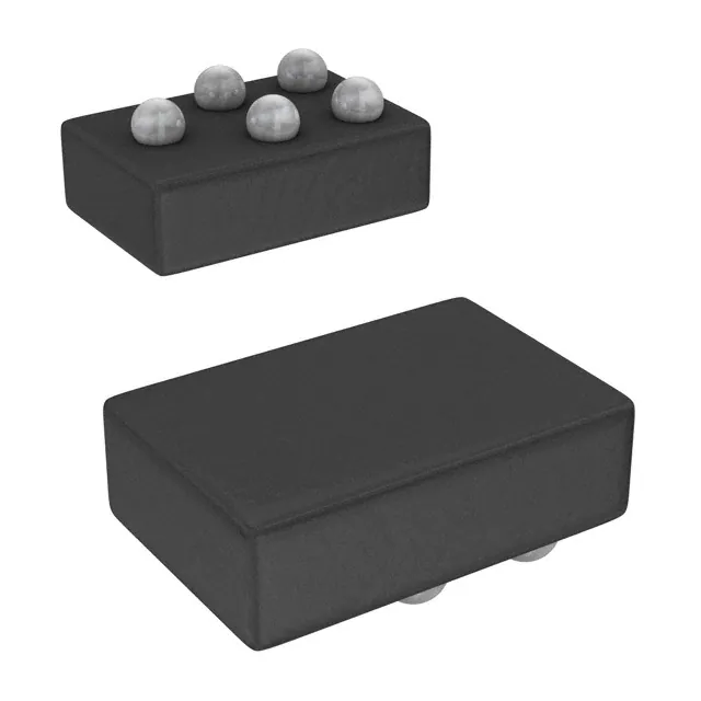
Lead-free Flip-Chip (5 bumps) package
The device uses STMicroelectronics’ IPD
technology on a non-conductive glass substrate
to optimize RF performance.
Features
STMicroelectronics BAL-NRF01D3 is an
ultraminiature balun. The device integrates
matching network and harmonics filter. Matching
impedance has been customized for the following
Nordic Semiconductor circuits: nRF24LE1 QFN32 pins, nRF24AP2-1CH, nRF24AP2-8CH,
nRF51422-QFAA (build code CA/C0),
nRF51822-QFAA (build code CA/C0) and
nRF51822-QFAB (build code AA/A0).
50 Ω nominal input / conjugate match to
Nordic Semiconductor chips nRF24LE1
QFN32, nRF24AP2-1CH, nRF24AP2-8CH,
nRF51422-QFAA (build code CA/C0),
nRF51822-QFAA (build code CA/C0) and
nRF51822-QFAB (build code AA/A0)
Low insertion loss
Low amplitude imbalance
Low phase imbalance
Small footprint < 1.5 mm2
The BAL-NRF01D3 has been tested and
approved by Nordic Semiconductor in their
nRF2723 and nRF2752 nRFgo modules.
Figure 1: Application schematic
3
DIFF
2
1
A
GND
SE
Benefits
Very low profile < 595 μm after reflow
High RF performance
RF BOM and area reduction
DIFF
VCC
B
C
Applications
2.45 GHz impedance matched balun filter
Optimized for Nordic's chip set
nRF24LE1/AP2, nRF51422-QFAA (build
code CA/C0), nRF51822-QFAA (build code
CA/C0) and nRF51822-QFAB (build code
AA/A0)
June 2017
DocID023215 Rev 7
This is information on a product in full production.
1/10
www.st.com
�Characteristics
1
BAL-NRF01D3
Characteristics
Table 1: Absolute maximum ratings (limiting values)
Value
Symbol
Parameter
Unit
Min.
PIN
VESD
TOP
Typ.
Max.
-
20
Input power RFIN
ESD ratings MIL STD883C
(HBM: C = 100 pF, R = 1.5 Ω, air discharge)
2000
ESD ratings charge device model
(JESD22-C101-C)
500
ESD ratings machine model
(MM: C = 200 pF, R = 25 W, L = 500 nH)
200
-
Operating temperature
-40
-
dBm
V
+105
°C
Table 2: Impedances (Tamb = 25 °C)
Value
Symbol
Parameter
Unit
Min.
Typ.
Max.
-
Ω
-
Ω
ZOUT
Nominal differential output
impedance
-
Conjugate match to:
nRF24LE1/AP2
nRF51422-QFAA (build code
CA/C0)
nRF51822-QFAA (build code
CA/C0)
nRF51822-QFAB (build code
AA/A0)
ZIN
Nominal input impedance
-
50
Table 3: RF performance (Tamb = 25 °C)
Value
Symbol
Parameter
Test condition
Unit
Min.
2/10
F
Frequency range (bandwidth) 2400 2540
Typ.
2400
Max.
2540
MHz
IL
Insertion loss in bandwidth
2.25
dB
RL
Return loss in bandwidth
10
dB
ɸimb
Phase imbalance
3
°
Aimb
Amplitude imbalance
0.1
dB
2f0
2nd harmonic filtering
4880 MHz
10
dB
3f0
3rd harmonic filtering
7320 MHz
20
dB
DocID023215 Rev 7
�BAL-NRF01D3
1.1
Characteristics
RF measurement
Figure 2: Transmission (Tamb = 25 °C)
Figure 3: Return loss on SE port (Tamb = 25 °C)
Figure 4: Return loss on DIFF port (Tamb = 25 °C)
Figure 5: Amplitude imbalance (Tamb = 25 °C)
Figure 6: Phase imbalance (Tamb = 25 °C)
DocID023215 Rev 7
3/10
�Application information
2
BAL-NRF01D3
Application information
Figure 7: Application schematic (courtesy of Nordic Semiconductor)
BAL-NRF01D3
Figure 8: nRF2723 application board (courtesy of Nordic Semiconductor)
4/10
DocID023215 Rev 7
�Application information
BAL-NRF01D3
Figure 9: nRF2752 application board (courtesy of Nordic Semiconductor)
BAL-NRF01D3
DocID023215 Rev 7
5/10
�Package information
3
BAL-NRF01D3
Package information
In order to meet environmental requirements, ST offers these devices in different grades of
ECOPACK® packages, depending on their level of environmental compliance. ECOPACK®
specifications, grade definitions and product status are available at: www.st.com.
ECOPACK® is an ST trademark.
3.1
Epoxy meets UL94, V0
Lead-free package
Flip-Chip 5 bumps package information
Figure 10: Flip-Chip 5 bumps package outline
X
B1
T
GND
D
Y
B
DIFF
SE
B2
VCC
B1
DIFF
A1
A
A2
A1
T1
H
Table 4: Flip-Chip 5 bumps dimensions
Parameter
6/10
Description
Min.
Typ.
Max.
Unit
X
X dimension of the die
1445
1485
1525
mm
Y
Y dimension of the die
980
1020
1060
mm
A
X pitch
604
mm
B
Y pitch
500
mm
A1
Distance from bump to edge of die on X axis
224
mm
B1
Distance from bump to edge of die on Y axis
260
mm
A2
Distance from VCC bump to SE bump on X axis
433
mm
B2
Distance from bump to edge of die on Y axis
510
mm
C
GND, VCC bump to SE bump pitch
500
mm
D
Bump diameter
T1
Substrate thickness
425
mm
H
Bump height
205
mm
T
Total die thickness
240
DocID023215 Rev 7
570
255
630
260
690
mm
�Package information
BAL-NRF01D3
Figure 11: Footprint - 3 mils stencil -non solder
mask defined
Copper pad diameter:
220 µm recommended
180 µm minimum
260 µm maximum
Solder mask opening:
220 µm recommended
180 µm minimum
260 µm maximum
Solder mask opening:
320 µm recommended
300 µm minimum
340 µm maximum
Copper pad diameter:
320 µm recommended
300 µm minimum
Solder stencil opening:
220 µm recommended
Solder stencil opening:
220 µm recommended
Figure 13: Footprint - 5 mils stencil -non solder
mask defined
Figure 14: Footprint - 5 mils stencil - solder mask
defined
Copper pad diameter:
220 µm recommended
180 µm minimum
260 µm maximum
Solder mask opening:
220 µm recommended
180 µm minimum
260 µm maximum
Solder mask opening:
320 µm recommended
300 µm minimum
340 µm maximum
Copper pad diameter:
320 µm recommended
300 µm minimum
Solder stencil opening:
330 µm recommended*
Solder stencil opening:
330 µm recommended*
*depending on paste, it can go down to 270 µm
3.2
Figure 12: Footprint - 3 mils stencil - solder mask
defined
*depending on paste, it can go down to 270 µm
Flip-chip 5 bumps packing information
Figure 15: Marking
Dot, ST logo
ECOPACK grade
xx = marking
z = manufacturing
location
yww = datecode
DocID023215 Rev 7
x x z
y ww
7/10
�Package information
BAL-NRF01D3
Figure 16: Flip Chip tape and reel specifications
More packing information is available in the application note:
8/10
AN2348 Flip-Chip: “Package description and recommendations for use”
AN4111: “BAL-NRF01D3 matched balun with integrated harmonics filter for
Nordic Semiconductor chips with ultralow power transceivers”
DocID023215 Rev 7
�Ordering information
BAL-NRF01D3
4
Ordering information
Table 5: Ordering information
5
Order code
Marking
Package
Weight
Base qty.
Delivery mode
BAL-NRF01D3
SC
Flip-Chip package (5 bumps)
1.82 mg
5000
Tape and reel
Revision history
Table 6: Document revision history
Date
Revision
Changes
15-Oct-2012
1
First issue.
13-Nov-2012
2
Added references to nRF51 series. Added Figure 9. Updated y-axis
labels in Figure 2.
04-Mar-2013
3
Updated footprint illustrations in Figure 13, and Figure 14.
06-Aug-2013
4
Added dimensions in Figure 10. Updated marking orientation in Figure
11 and Figure 12.
13-Jan-2014
5
Updated document title and product references.
07-Jul-2015
6
Updated Table 1.
21-Jun-2017
7
Updated Figure 10: "Flip-Chip 5 bumps package outline" and Table 4:
"Flip-Chip 5 bumps dimensions".
DocID023215 Rev 7
9/10
�BAL-NRF01D3
IMPORTANT NOTICE – PLEASE READ CAREFULLY
STMicroelectronics NV and its subsidiaries (“ST”) reserve the right to make changes, corrections, enhancements, modifications, and
improvements to ST products and/or to this document at any time without notice. Purchasers should obtain the latest relevant information on ST
products before placing orders. ST products are sold pursuant to ST’s terms and conditions of sale in place at the time of order
acknowledgement.
Purchasers are solely responsible for the choice, selection, and use of ST products and ST assumes no liability for application assistance or the
design of Purchasers’ products.
No license, express or implied, to any intellectual property right is granted by ST herein.
Resale of ST products with provisions different from the information set forth herein shall void any warranty granted by ST for such product.
ST and the ST logo are trademarks of ST. All other product or service names are the property of their respective owners.
Information in this document supersedes and replaces information previously supplied in any prior versions of this document.
© 2017 STMicroelectronics – All rights reserved
10/10
DocID023215 Rev 7
�
很抱歉,暂时无法提供与“BAL-NRF01D3”相匹配的价格&库存,您可以联系我们找货
免费人工找货- 国内价格 香港价格
- 41+1.9129741+0.22720
- 100+1.88348100+0.22370
- 250+1.85276250+0.22005
- 500+1.82328500+0.21655
- 1000+1.793791000+0.21304
- 3000+1.329093000+0.15785
- 国内价格 香港价格
- 5000+1.289835000+0.15319
- 10000+1.2798310000+0.15200
- 15000+1.2698315000+0.15082
- 20000+1.2598320000+0.14963
- 25000+1.2398425000+0.14725
- 国内价格 香港价格
- 5000+1.369825000+0.16269
- 10000+1.3498210000+0.16032
- 15000+1.3398215000+0.15913
- 20000+1.3335020000+0.15838
- 25000+1.3198325000+0.15675


 工商网监
湘ICP备2023018690号
工商网监
湘ICP备2023018690号
