BALF-ATM-01E3
50 ohms / matched to ATSAMR21E18 balun transformer, with
integrated harmonic filter
Datasheet - production data
Description
The BALF-ATM-01E3 from STMicroelectronics is
an integrated balun, which also integrates a
matching network in a monolithic glass substrate.
Matching impedance has been customized for
the ATMEL chip. The device uses
STMicroelectronics’ IPD technology on a nonconductive glass substrate to optimize RF
performance.
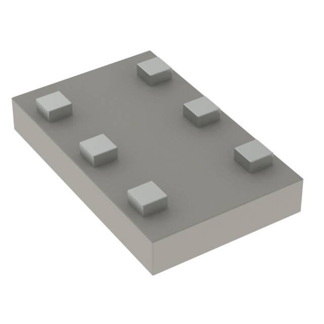
Coated CSP on glass bumpless
Figure 1: Pin configuration (pad view)
Features
2.4 – 2.5 GHz balun with integrated
matching network
Matching optimized for following chipsets:
ATSAMR21E18
Low insertion loss
Low amplitude imbalance
Low phase imbalance
Coated CSP on glass bumpless
Small footprint 2.5 mm²
BAL+
GND
GND
BAL-
GND
SE
PAD VIEW
Benefits
Very low profile
High RF performance
PCB space saving versus discrete solution
BOM count reduction
Efficient manufacturability
June 2017
DocID030654 Rev 1
This is information on a product in full production.
1/12
www.st.com
�Characteristics
1
BALF-ATM-01E3
Characteristics
Table 1: Absolute maximum ratings (limiting values)
Value
Symbol
Parameter
Unit
Min.
PIN
VESD
TOP
Input power RFIN
Typ.
Max.
-
4
ESD ratings MIL STD883C
(HBM: C = 100 pF, R = 1.5 Ω, air discharge)
2000
ESD ratings machine model
(MM: C = 200 pF, R = 25 W, L = 500 nH)
500
-
Operating temperature
-40
-
dBm
V
+105
°C
Table 2: Electrical characteristics (Tamb = 25 °C)
Value
Symbol
Parameter
Unit
Min.
ZOUT
ZIN
2/12
Nominal differential output impedance
Typ.
Max.
Conjugate match to ATSAMR21E18
Ω
50
Nominal input impedance
f
Frequency range (bandwidth)
IL
Insertion loss at 2.45 GHz
RL
Single ended side at 2.45 GHz
15
26.3
dB
RL
Differential side at 2.45 GHz
15
26.1
dB
ɸimb
Phase imbalance at 2.45 GHz
-9
0
9
°
Aimb
Amplitude imbalance at 2.45 GHz
-0.4
0
0.4
dB
H2
Harmonic 2 attenuation at 4.9 GHz
20
35
dB
H3
Harmonic 3 attenuation at 7.35 GHz
20
25
dB
DocID030654 Rev 1
2400
Ω
0.91
2500
MHz
1.3
dB
�BALF-ATM-01E3
1.1
Characteristics
RF measurement
Figure 2: Transmission (dB)
Figure 3: Insertion loss (dB)
Transmission (dB)
(dB)
0
0.0
-0.2
-10
-0.4
-20
-0.6
-0.8
-30
-1.0
-40
-1.2
F(GHz)
-50
0
2
4
6
8
F(GHz)
-1.4
10
2.40 2.41 2.42 2.43 2.44 2.45
Figure 4: H2 attenuation (dB)
2.46 2.47 2.48 2.49 2.50
Figure 5: H3 attenuation (dB)
H2 (dB)
H3 (dB)
0
0
-10
-10
-20
-20
-30
-30
-40
-40
F(GHz)
-50
4.80 4.82 4.84 4.86 4.88 4.90
4.92 4.94 4.96 4.98 5.00
F(GHz)
-50
7.20
Figure 6: Return Loss SE (dB)
7.25
7.30
7.35
7.40
7.45
7.50
Figure 7: Return Loss diff (dB)
Return loss SE (dB)
0
0
Return loss diff (dB)
-10
-10
-20
-20
-30
-30
-40
F(GHz)
2.40 2.41 2.42 2.43 2.44 2.45
F(GHz)
-50
-40
2.46 2.47 2.48 2.49 2.50
2.40
DocID030654 Rev 1
2.41 2.42
2.43 2.44 2.45
2.46 2.47
2.48 2.49 2.50
3/12
�Characteristics
BALF-ATM-01E3
Figure 8: Amplitude imbalance (dB)
Figure 9: Phase imbalance (°)
1.0 Amplitude imbalance (dB)
0.8
15
Phase imbalance (°)
0.6
10
0.4
0.2
5
-0.0
0
-0.2
-0.4
-5
-0.6
-10
-0.8
F(GHz)
-1.0
2.40
4/12
F(GHz)
-15
2.41 2.42
2.43 2.44 2.45
2.46 2.47
2.48 2.49 2.50
2.40
DocID030654 Rev 1
2.41
2.42
2.43 2.44
2.45 2.46
2.47
2.48
2.49 2.50
�Application schematic
BALF-ATM-01E3
Application schematic
PB22
PB23
PA27
RESETN
PA28
GND
VDDCORE
PA00
VDDIN
SWCLK
SWDIO
PB02
PB03
Figure 10: Application schematic
VDDIO
PA01
GND
GND
XTAL2
USB_DP
XTAL1
USB_DM
AGND
PA23
AVDD
PA22
ATSAMR21E18
AVDDOUT
VDDOUT
4
PA16
PA15
RFN
RFP
PA07
RFCTRL4
PA17
RFCTRL3
PA06
RFCTRL2
PA18
AGND_RFN
PA05
AGND_RFP
PA19
RFCTRL1
PA04
RFCTRL0
GND
GND
AGND
VDDIO
2
3
BALFATM01E3
2
5
6
Antenna
(50Ω)
1
DocID030654 Rev 1
5/12
�Package information
3
BALF-ATM-01E3
Package information
In order to meet environmental requirements, ST offers these devices in different grades of
ECOPACK® packages, depending on their level of environmental compliance. ECOPACK®
specifications, grade definitions and product status are available at: www.st.com.
ECOPACK® is an ST trademark.
3.1
Coated CSP on glass bumpless package information
Figure 11: Coated CSP on glass bumpless package outline
T
L
c
W
a
d
b
PAD VIEW
Table 3: Coated CSP on glass bumpless dimensions
Dimensions (in mm)
Parameter
6/12
Min.
Typ.
Max.
L
1.900
2.000
2.100
W
1.150
1.250
1.350
T
0.395
0.425
0.455
a
0.200
b
0.200
c
0.884
d
0.650
DocID030654 Rev 1
�Package information
BALF-ATM-01E3
Figure 12: Recommended balun land pattern
350µm
Figure 13: PCB stackup
Solder resist:
20 µm
180µm
Finished copper:
85 µm
(copper 70 µm + plating 15 µm)
SE
1000µm
GND
BAL-
1000µm
300µm
180µm
800µm
200µm
300µm
200µm
600µm
GND
GND
BAL+
180µm
GND plane
Prepreg:
180 µm
Copper:
35 µm
Figure 14: Marking
Figure 15: Pad bottom view
ECOPACK grade
BAL+
GND
GND
BAL-
GND
SE
XX: marking
X
X
Z
y
w
w
Z: manufacturing location
yww: datecode
PAD VIEW
Table 4: Pin description
Description
Pad#
Name
1
SE
2, 5, 6
GND
Ground connection
3
BAL-
Balun differential negative pin
4
BAL+
Balun differential positive pin
Single ended antenna connection
DocID030654 Rev 1
7/12
�Package information
3.2
BALF-ATM-01E3
Coated CSP on glass bumpless packing information
Figure 16: Tape mechanical data
P0
Ø D0
F
W
+
K0
+
+
P1
+
P2
Ø D1
User direction of unreeling
Note:
Pocket dimensions are not on scale
Pocket shape may vary depending on package
Table 5: Tape dimension definitions
Dimesions (in mm)
Ref.
8/12
Min.
Typ.
Max.
P1
3.90
4.00
4.10
P0
3.90
4.00
4.10
D0
1.40
1.50
1.60
D1
0.35
0.40
0.45
F
3.45
3.50
3.55
K0
0.47
0.52
0.57
P2
1.95
2.00
2.05
W
7.90
8.00
8.30
DocID030654 Rev 1
�Package information
BALF-ATM-01E3
Figure 17: Package orientation in reel
Pin 1 located according to EIA-481
Note:
3.3
Pocket dimensions are not on scale
Pocket shape may vary depending on package
Stencil opening design
Figure 18: Stencil opening in mm
200µm
200µm
stencil opening
footprint
3.4
Solder paste
1.
2.
3.
4.
5.
100 µm Solder stencil thickness is recommended
Halide-free flux qualification ROL0 according to ANSI/J-STD-004.
“No clean” solder paste is recommended.
Offers a high tack force to resist component movement during high speed.
Solder paste with fine particles: powder particle size is 20-45 µm.
DocID030654 Rev 1
9/12
�Package information
3.5
Placement
1.
2.
3.
4.
5.
6.
10/12
BALF-ATM-01E3
Manual positioning is not recommended.
It is recommended to use the lead recognition capabilities of the placement system,
not the outline centering
Standard tolerance of ±0.05 mm is recommended.
3.5 N placement force is recommended. Too much placement force can lead to
squeeze out solder paste and cause solder joints to short. Too low placement force
can lead to insufficient contact between package and solder paste that could cause
open solder joints or badly centered packages.
To improve the package placement accuracy, a bottom side optical control should be
performed with a high resolution tool.
For assembly, a perfect supporting of the PCB (all the more on flexible PCB) is
recommended during solder paste printing, pick and place and reflow soldering by
using optimized tools.
DocID030654 Rev 1
�Ordering information
BALF-ATM-01E3
4
Ordering information
Figure 19: Ordering information scheme
BALF – ATM – 01 E3
Balun with filter
Compatible with an Atmel Chip
01: version (compatible with ATSAMR21E18)
E3: Coated CSP on glass bumpless
Table 6: Ordering information
5
Order code
Marking
Package
Weight
Base
qty.
Delivery mode
BALF-ATM-01E3
TJ
Coated CSP on glass
bumpless
2.28 mg
5000
Tape and reel
(7'')
Revision history
Table 7: Document revision history
Date
Revision
07-Jun-2017
1
Changes
Initial release.
DocID030654 Rev 1
11/12
�BALF-ATM-01E3
IMPORTANT NOTICE – PLEASE READ CAREFULLY
STMicroelectronics NV and its subsidiaries (“ST”) reserve the right to make changes, corrections, enhancements, modifications, and
improvements to ST products and/or to this document at any time without notice. Purchasers should obtain the latest relevant information on ST
products before placing orders. ST products are sold pursuant to ST’s terms and conditions of sale in place at the time of order
acknowledgement.
Purchasers are solely responsible for the choice, selection, and use of ST products and ST assumes no liability for application assistance or the
design of Purchasers’ products.
No license, express or implied, to any intellectual property right is granted by ST herein.
Resale of ST products with provisions different from the information set forth herein shall void any warranty granted by ST for such product.
ST and the ST logo are trademarks of ST. All other product or service names are the property of their respective owners.
Information in this document supersedes and replaces information previously supplied in any prior versions of this document.
© 2017 STMicroelectronics – All rights reserved
12/12
DocID030654 Rev 1
�
很抱歉,暂时无法提供与“BALF-ATM-01E3”相匹配的价格&库存,您可以联系我们找货
免费人工找货