®
BC547B BC547C
SMALL SIGNAL NPN TRANSISTORS
T ype BC547B BC547C
s
Marking BC547B BC547C
s
s
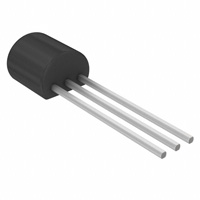
SILICON EPITAXIAL PLANAR NPN TRANSISTORS TO-92 PACKAGE SUITABLE FOR THROUGH-HOLE PCB ASSEMBLY BC547B - THE PNP COMPLEMENTARY TYPE IS BC557B TO-92
s
APPLICATIONS s WELL SUITABLE FOR TV AND HOME APPLIANCE EQUIPMENT s SMALL LOAD SWITCH TRANSISTORS WITH HIGH GAIN AND LOW SATURATION VOLTAGE
INTERNAL SCHEMATIC DIAGRAM
ABSOLUTE MAXIMUM RATINGS
Symbol V CBO V CEO V EBO IC I CM P tot T stg Tj Parameter Collector-Base Voltage (I E = 0 ) Collector-Emitter Voltage (I B = 0 ) Emitter-Base Voltage (I C = 0 ) Collector Current Collector Peak Current Total Dissipation at T C = 2 5 o C Storage Temperature Max. Operating Junction Temperature Value 50 45 6 100 200 500 -65 to 150 150 Unit V V V mA mA mW
o o
C C
January 2003
1/4
�BC547B / BC547C
THERMAL DATA
R thj-amb • Thermal Resistance Junction-Ambient R thj-Case • Thermal Resistance Junction-Case Max Max 250 83.3
o o
C/W C/W
ELECTRICAL CHARACTERISTICS (Tcase = 25 oC unless otherwise specified)
Symbol I CBO I EBO Parameter Collector Cut-off Current (I E = 0 ) Emitter Cut-off Current (I C = 0 ) Test Conditions V CB = 3 0 V V CB = 3 0 V V EB = 5 V I C = 1 0 mA 45 T C = 1 50 o C Min. Typ. Max. 15 5 100 Unit nA µA nA V
V (BR)CEO ∗ Collector-Emitter Breakdown Voltage (I B = 0 ) V CE(sat) ∗ V BE(sat) ∗ V BE(on) ∗ h FE Collector-Emitter Saturation Voltage Base-Emitter Saturation Voltage Base-Emitter On Voltage DC Current Gain
I C = 1 0 mA I C = 1 00 mA I C = 1 0 mA I C = 1 00 mA IC = 2 mA I C = 1 0 mA IC = 2 mA for B C547B for B C547C
I B = 0 .5 mA IB = 5 m A I B = 0 .5 mA IB = 5 m A V CE = 5 V V CE = 5 V V CE = 5 V 200 420 100 0.58
0.09 0.2 0.7 0.9 0.66
0.25 0.6
V V V V
0.7 0.77 450 800
V V
fT C CBO C EBO NF
Transition Frequency Collector-Base Capacitance Emitter-Base Capacitance Noise Figure
I C = 1 0 mA V CE = 5 V f = 1 00MHz IE = 0 IC = 0 V CB = 1 0 V V EB = 0 .5 V f = 1 MHz f = 1 MHz
MHz 1.5 11 2 10 pF pF dB
V CE = 5 V IC = 2 00 µ A f = 1KHz ∆ f = 200 Hz R G = 2 K Ω
∗ Pulsed: Pulse duration = 300 µs, duty cycle ≤ 2 %
2/4
�BC547B / BC547C
TO-92 MECHANICAL DATA
mm MIN. A b D E e e1 L R S1 W V 4.32 0.36 4.45 3.30 2.41 1.14 12.70 2.16 1.14 0.41 4 degree TYP. MAX. 4.95 0.51 4.95 3.94 2.67 1.40 15.49 2.41 1.52 0.56 6 degree MIN. 0.170 0.014 0.175 0.130 0.095 0.045 0.500 0.085 0.045 0.016 4 degree inch TYP. MAX. 0.195 0.020 0.194 0.155 0.105 0.055 0.609 0.094 0.059 0.022 6 degree
DIM.
3/4
�BC547B / BC547C
Information furnished is believed to be accurate and reliable. However, STMicroelectronics assumes no responsibility for the consequences of use of such information nor for any infringement of patents or other rights of third parties which may result from its use. No license is granted by implication or otherwise under any patent or patent rights of STMicroelectronics. Specification mentioned in this publication are subject to change without notice. This publication supersedes and replaces all information previously supplied. STMicroelectronics products are not authorized for use as critical components in life support devices or systems without express written approval of STMicroelectronics. The ST logo is a trademark of STMicroelectronics © 2002 STMicroelectronics – Printed in Italy – All Rights Reserved STMicroelectronics GROUP OF COMPANIES Australia - Brazil - Canada - China - Finland - France - Germany - Hong Kong - India - Israel - Italy - Japan - Malaysia - Malta - Morocco Singapore - Spain - Sweden - Switzerland - United Kingdom - United States. http://www.st.com
4/4
�
很抱歉,暂时无法提供与“BC547C”相匹配的价格&库存,您可以联系我们找货
免费人工找货