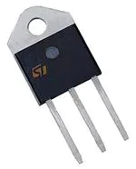
BTW67
Datasheet
50 A,1000 V SCR thyristor in RD91
Features
A
•
•
•
•
G
K
•
High current SCR
High commutation capability
Low thermal resistance with clip bonding
Insulated package RD91 high power:
–
Low thermal resistance with clip bonding
–
Insulated voltage: 2500 VRMS
–
Complies with UL 1557 (File ref : E81734)
RoHS (2002/95/EC) compliant
Applications
RD91
•
•
•
Solid state relays
Welding equipment
High power motor control
Description
Available in 2500 V insulated high power package, the 50 A and 1000 V SCR BTW67
is suitable in applications where power handling and power dissipation are critical,
such as solid state relays, welding equipment and high power motor control.
Product status link
Based on a clip assembly technology, they offer a superior performance in surge
current handling capabilities.
BTW67
Product summary
IT(RMS)
50 A
VDRM/VRRM
1000 V
IGT
80 mA
DS0642 - Rev 6 - June 2019
For further information contact your local STMicroelectronics sales office.
www.st.com
�BTW67
Characteristics
1
Characteristics
Table 1. Absolute maximum ratings
Symbol
Parameters
IT(RMS)
RMS on-state current (full sine wave)
Average on-state current
IT(AV)
(180° conduction angle)
ITSM
Non repetitive surge peak on-state current (full cycle, Tj initial = 25 °C)
I2t
Value
Unit
Tc = 70 °C
50
A
Tc = 70 °C
32
A
tp =8.3 ms
610
A
1680
A2s
tp = 10 ms
I2t value for fusing
Critical rate of rise of on-state current
F = 60 Hz
Tj = 125 °C
50
A/µs
tp = 20 µs
Tj = 125 °C
8
A
Tj = 125 °C
1
W
Storage junction temperature range
-40 to +150
°C
Tj
Operating junction temperature range
-40 to +125
°C
VGRM
Maximum peak reverse gate voltage
5
V
2500
V
dl/dt
IG = 2 x IGT , tr ≤ 100 ns
IGM
Peak gate current
PG(AV)
Average gate power dissipation
Tstg
Vins
Insulation RMS voltage, 1 minute
Table 2. Electrical characteristics (Tj = 25°C, unless otherwise specified)
Symbol
IGT
Tj
Test conditions
VD = 12 V, RL = 33 Ω
25 °C
VGT
Value
Unit
Min.
8
Max
80
Max
1.3
V
Min.
0.2
V
mA
VGD
VD = VDRM, RL = 3.3 kΩ
IH
IT = 500 mA, gate open
Max.
150
mA
IL
IG = 1.2 x IGT
Max.
200
mA
125 °C
dV/dt
VD = 67 %, VDRM gate open
125 °C
Min.
1000
V/µs
VTM
ITM = 100 A, tp = 380 μs
25 °C
Max.
1.9
V
VTO
threshold on-state voltage
125 °C
Max.
1.0
V
RD
Dynamic resistance
125 °C
Max.
8.5
mΩ
10
µA
5
mA
IDRM/IRRM
25 °C
VD = VDRM, VR = VRRM
125 °C
Max.
Table 3. Thermal resistance
Symbol
Rth(j-c)
DS0642 - Rev 6
Parameters
Junction to case (D.C)
Value
Unit
1.0
°C/W
page 2/10
�BTW67
Characteristics (curves)
1.1
Characteristics curves
Figure 1. Maximum average power dissipation versus
average on-state current
Figure 2. Average on-state current versus case
temperature
IT(AV) (A)
P(W)
55
60
α = 180°
50
DC
50
45
40
40
35
α = 180°
30
30
25
20
20
15
360°
360°
10
10
IT(AV) (A)
5
0
0
20
10
40
30
Figure 3. Relative variation of thermal impedance versus
pulse duration
1.E-00
Tc(°C)
0
0
25
50
75
100
125
Figure 4. Relative variation of gate trigger current, holding
current and latching current versus junction temperature
IGT,IH,IL[Tj] / IGT,IH,IL[Tj = 25 °C]
K = [Zth/ Rth]
2.5
2.0
IGT
1.E-01
1.5
Zth(j-c)
1.0
IH and IL
0.5
Tj (°C)
tP(s)
1.E-02
1.E-03
1.E-01
1.E+01
1.E+03
Figure 5. Surge peak on-state current versus number of
cycles
0.0
-40
110
Figure 6. Non repetitive surge peak on-state current for a
sinusoidal pulse with width tp
很抱歉,暂时无法提供与“BTW69-200RG”相匹配的价格&库存,您可以联系我们找货
免费人工找货