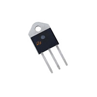
BTW67
Datasheet
50 A,1000 V SCR thyristor in RD91
A
Features
K
•
•
•
•
G
A
G
K
•
High current SCR
High commutation capability
Low thermal resistance with clip bonding
Insulated package RD91 high power:
–
Low thermal resistance with clip bonding
–
Insulated voltage: 2500 VRMS
–
Complies with UL 1557 (File ref : E81734)
RoHS (2002/95/EC) compliant
Applications
RD91
•
•
•
Product status link
BTW67
Product summary
IT(RMS)
50 A
VDRM/VRRM
1000 V
IGT
80 mA
Solid state relays
Welding equipment
High power motor control
Description
Available in 2500 V insulated high power package, the 50 A and 1000 V SCR BTW67
is suitable in applications where power handling and power dissipation are critical,
such as solid state relays, welding equipment and high power motor control.
Based on a clip assembly technology, they offer a superior performance in surge
current handling capabilities.
DS0642 - Rev 7 - February 2023
For further information contact your local STMicroelectronics sales office.
www.st.com
�BTW67
Characteristics
1
Characteristics
Table 1. Absolute maximum ratings
Symbol
Parameters
IT(RMS)
RMS on-state current (full sine wave)
Average on-state current
IT(AV)
(180° conduction angle)
ITSM
Non repetitive surge peak on-state current (full cycle, Tj initial = 25 °C)
I2t
Value
Unit
Tc = 70 °C
50
A
Tc = 70 °C
32
A
tp =8.3 ms
610
A
1680
A2s
tp = 10 ms
I2t value for fusing
Critical rate of rise of on-state current
F = 60 Hz
Tj = 125 °C
50
A/µs
tp = 20 µs
Tj = 125 °C
8
A
Tj = 125 °C
1
W
Storage junction temperature range
-40 to +150
°C
Tj
Operating junction temperature range
-40 to +125
°C
VGRM
Maximum peak reverse gate voltage
5
V
2500
V
dl/dt
IG = 2 x IGT , tr ≤ 100 ns
IGM
Peak gate current
PG(AV)
Average gate power dissipation
Tstg
Vins
Insulation RMS voltage, 1 minute
Table 2. Electrical characteristics (Tj = 25°C, unless otherwise specified)
Symbol
IGT
Tj
Test conditions
VD = 12 V, RL = 33 Ω
25 °C
VGT
Value
Unit
Min.
8
Max
80
Max
1.3
V
Min.
0.2
V
mA
VGD
VD = VDRM, RL = 3.3 kΩ
IH
IT = 500 mA, gate open
Max.
150
mA
IL
IG = 1.2 x IGT
Max.
200
mA
125 °C
dV/dt
VD = 67 %, VDRM gate open
125 °C
Min.
1000
V/µs
VTM
ITM = 100 A, tp = 380 μs
25 °C
Max.
1.9
V
VTO
threshold on-state voltage
125 °C
Max.
1.0
V
RD
Dynamic resistance
125 °C
Max.
8.5
mΩ
10
µA
5
mA
IDRM/IRRM
25 °C
VD = VDRM, VR = VRRM
125 °C
Max.
Table 3. Thermal resistance
Symbol
Rth(j-c)
DS0642 - Rev 7
Parameters
Junction to case (D.C)
Value
Unit
1.0
°C/W
page 2/9
�BTW67
Characteristics curves
1.1
Characteristics curves
Figure 1. Maximum average power dissipation versus
average on-state current
Figure 2. Average on-state current versus case
temperature
IT(AV) (A)
P(W)
55
60
α = 180°
50
DC
50
45
40
40
35
α = 180°
30
30
25
20
20
15
360°
360°
10
10
IT(AV) (A)
5
0
0
20
10
40
30
Figure 3. Relative variation of thermal impedance versus
pulse duration
1.E-00
Tc(°C)
0
0
25
50
75
100
125
Figure 4. Relative variation of gate trigger current, holding
current and latching current versus junction temperature
IGT,IH,IL[Tj] / IGT,IH,IL[Tj = 25 °C]
K = [Zth/ Rth]
2.5
2.0
IGT
1.E-01
1.5
Zth(j-c)
1.0
IH and IL
0.5
Tj (°C)
tP(s)
1.E-02
1.E-03
1.E-01
1.E+01
1.E+03
Figure 5. Surge peak on-state current versus number of
cycles
0.0
-40
110
Figure 6. Non repetitive surge peak on-state current for a
sinusoidal pulse with width tp
很抱歉,暂时无法提供与“BTW69-600RG”相匹配的价格&库存,您可以联系我们找货
免费人工找货