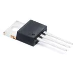
BUL3N7
MEDIUM VOLTAGE FAST-SWITCHING NPN POWER TRANSISTOR
Features
■ ■ ■ ■
MEDIUM VOLTAGE CAPABILITY LOW SPREAD OF DYNAMIC PARAMETERS MINIMUM LOT-TO-LOT SPREAD FOR RELIABLE OPERATION VERY HIGH SWITCHING SPEED
2 3
Applications
■
1
ELECTRONIC BALLASTS FOR FLUORESCENT LIGHTING
TO-220
Description
The BUL3N7 is manufactured using high voltage Multi-Epitaxial Planar technology for high switching speeds and medium voltage capability. It uses a Cellular Emitter structure with planar edge termination to enhance switching speeds while maintaining the wide RBSOA. The device is expressly designed for a new solution to be used in compact fluorescent lamps, H.F. ballast voltage FED where it is coupled with the BUL3P5, its complementary PNP transistor.
Internal Schematic Diagram
Order Codes
Part Number BUL3N7 Marking BUL3N7 Package TO-220 Packing TUBE
December 2005
rev.1 1/10
www.st.com 10
�1 Absolute Maximum Ratings
BUL3N7
1
Table 1.
Symbol VCES VCEO VEBO IC ICM IB IBM PTOT Tstg TJ
Absolute Maximum Ratings
Absolute Maximum Rating
Parameter Collector-Emitter Voltage (VBE = 0) Collector-Emitter Voltage (IB = 0) Emitter-Base Voltage (IC = 0, IB = -0.75 A, tp < 100ms, Tj < 150°C) Collector Current Collector Peak Current (tP < 5ms) Base Current Base Peak Current (tP < 5ms) Total dissipation at Tc = 25°C Storage Temperature Max. Operating Junction Temperature Value 700 400 V(BR)EBO 3 6 1.5 3 60 -65 to 150 150 Unit V V V A A A A W °C °C
Table 2.
Symbol RthJ-case RthJ-amb
Thermal Data
Parameter Thermal Resistance Junction-Case_______________Max Thermal Resistance Junction-Ambient ______ ______Max Value 2.08 62.5 Unit °C/W °C/W
2/10
�BUL3N7
2 Electrical Characteristics
2
Table 3.
Symbol ICES
Electrical Characteristics
Electrical Characteristics (TCASE = 25°C; unless otherwise specified)
Parameter Collector Cut-off Current (V BE = 0) Test Conditions VCE = 700 V VCE = 700 V__ __TC = 125°C 10 400 0.5 0.5 1.1 1.2 1.3 10 18 4 Min. Typ. Max. 0.1 0.5 18 Unit mA mA V V V V V V V
V(BR)EBO Emitter-Base Breakdown Voltage IE = 10 mA (IC = 0) VCEO(sus) Collector-Emitter Note: 1 Sustaining Voltage (IB = 0) VCE(sat) Note: 1 VBE(sat) Note: 1 Collector-Emitter Saturation Voltage Base-Emitter Saturation Voltage IC = 100 mA IC = 0.7 A __ _ IB = 0.1A IC = 1 A __ _ IB = 0.2 A IC = 0.5A ____ IB = 0.1 A IC = 1A _____ IB = 0.2 A IC = 2A _____ IB = 0.4 A IC = 10 mA _ VCE = 5 V hFE DC Current Gain IC = 0.7A ____ VCE = 5 V IC = 2A_ VCE = 5 V IC = 0.7 A ___ V CC = 250 V
34
tr ts tf ts tf
RESISTIVE LOAD Rise Time Storage Time Fall Time INDUCTIVE LOAD Storage Time Fall Time
IB1 = 0.14 A __ IB2 = -0.14 A Tp = 30 µs IC = 1 A ____ VBE(off) = -5 V L = 1 mH IB1 = 0.2 A Rbb = 0 Ω Vclamp = 200 V
80 2.4 100 450 120
ns µs ns ns ns
Note: 1 Pulsed duration = 300 µs, duty cycle ≤1.5%.
3/10
�2 Electrical Characteristics
BUL3N7
2.1
Typical Characteristics
Safe Operating Area Figure 2. DC Current Gain
Figure 1.
Figure 3.
DC Current Gain
Figure 4.
Collector Emitter Saturation Voltage
Figure 5.
Base Emitter Saturation Voltage
Figure 6.
Switching Times Resistive Load
4/10
�BUL3N7
Figure 7. Switching Times Inductive Load Figure 8.
2 Electrical Characteristics
Reverse Bised SOA
5/10
�3 Test Circuits
BUL3N7
3
Figure 9.
Test Circuits
Inductive Load Switching Test Circuit
1) Fast Electronic Switching 2) Non-inductive Resisitor 3) Fast Recovery Rectifier
Figure 10. Resistive Load Switching Test Circuits
1) Fast Electronic Switching 2) Non-inductive Resisitor
6/10
�BUL3N7
4 Package Mechanical Data
4
Package Mechanical Data
In order to meet environmental requirements, ST offers these devices in ECOPACK® packages. These packages have a Lead-free second level interconnect . The category of second level interconnect is marked on the package and on the inner box label, in compliance with JEDEC Standard JESD97. The maximum ratings related to soldering conditions are also marked on the inner box label. ECOPACK is an ST trademark. ECOPACK specifications are available at: www.st.com
7/10
�4 Package Mechanical Data
BUL3N7
TO-220 MECHANICAL DATA
DIM. A b b1 c D E e e1 F H1 J1 L L1 L20 L30 mm. MIN. 4.40 0.61 1.15 0.49 15.25 10 2.40 4.95 1.23 6.20 2.40 13 3.50 16.40 28.90 3.75 2.65 3.85 2.95 0.147 0.104 TYP MAX. 4.60 0.88 1.70 0.70 15.75 10.40 2.70 5.15 1.32 6.60 2.72 14 3.93 MIN. 0.173 0.024 0.045 0.019 0.60 0.393 0.094 0.194 0.048 0.244 0.094 0.511 0.137 0.645 1.137 0.151 0.116 inch TYP. MAX. 0.181 0.034 0.066 0.027 0.620 0.409 0.106 0.202 0.052 0.256 0.107 0.551 0.154
øP
Q
8/10
�BUL3N7
5 Revision History
5
Revision History
Date 09-Dec-2005 Revision 1 Initial Relase Changes
9/10
�5 Revision History
BUL3N7
Information furnished is believed to be accurate and reliable. However, STMicroelectronics assumes no responsibility for the consequences of use of such information nor for any infringement of patents or other rights of third parties which may result from its use. No license is granted by implication or otherwise under any patent or patent rights of STMicroelectronics. Specifications mentioned in this publication are subject to change without notice. This publication supersedes and replaces all information previously supplied. STMicroelectronics products are not authorized for use as critical components in life support devices or systems without express written approval of STMicroelectronics. The ST logo is a registered trademark of STMicroelectronics. All other names are the property of their respective owners © 2005 STMicroelectronics - All rights reserved STMicroelectronics group of companies Australia - Belgium - Brazil - Canada - China - Czech Republic - Finland - France - Germany - Hong Kong - India - Israel - Italy - Japan Malaysia - Malta - Morocco - Singapore - Spain - Sweden - Switzerland - United Kingdom - United States of America www.st.com
10/10
�
很抱歉,暂时无法提供与“BUL3N7”相匹配的价格&库存,您可以联系我们找货
免费人工找货