®
BUX348
FAST-SWITCHING POWER TRANSISTOR
s
s s s s
STMicroelectronics PREFERRED SALESTYPE NPN TRANSISTOR HIGH VOLTAGE FAST SWITCHING OFF-LINE APPLICATIONS TO 380V
APPLICATIONS SWITCH MODE POWER SUPPLIES s UNINTERRUPTABLE POWER SUPPLY s DC AND AC MOTOR CONTROL
s
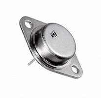
1 2
TO-3 (version "S")
INTERNAL SCHEMATIC DIAGRAM
ABSOLUTE MAXIMUM RATINGS
Symbol V CEV V CEO V EBO IC I CM IB I BM P tot T stg Tj Parameter Collector-Emitter Voltage (V BE = - 1.5 V) Collector-Emitter Voltage (I B = 0 ) Emitter-Base Voltage (I C = 0 ) Collector Current Collector Peak Current Base Current Base Peak Current (t p < 5 m s) Total Power Dissipation at T case ≤ 2 5 C
o
Value 850 450 7 45 60 9 15 300 -65 to 200 200
Unit V V V A A A A W
o o
Storage Temperature Junction Temperature
C C
March 2003
1/4
�BUX348
THERMAL DATA
R thj-case Thermal Resistance Junction-case Max 0.58
o
C/W
ELECTRICAL CHARACTERISTICS (Tcase = 25 oC unless otherwise specified)
Symbol I CER I CEV Parameter Collector Cut-off Current (R BE = 1 0 Ω ) Collector Cut-off Current (V BE = -1.5V) Emitter Cut-off Current (I C = 0) Test Conditions V CE = V CEV V CE = V CEV V CE = V CEV V CE = V CEV V EB = 5 V I C = 0 .2 A L = 25 mH 450 T c = 100 o C T c = 100 o C Min. Typ. Max. 0.4 2 0.4 2 2 Unit mA mA mA mA mA V
I EBO
V CEO(sus) ∗ Collector-Emitter Sustaining Voltage (I B = 0) V EBO V CE(sat) ∗ V BE(sat) ∗ di C /dt V CE(3 µ s) ∗ V CE(5 µ s) ∗ Emitter-Base Voltage (I C = 0 ) Collector-Emitter Saturation Voltage Base-Emitter Saturation Voltage Rated of Rise on-state Collector Current Collector-Emitter Dynamic Voltage Collector-Emitter Dynamic Voltage
I E = 1 00 mA IC = 30 A IC = 30 A IC = 30 A IC = 30 A IB = 6 A IB = 6 A IB = 6 A IB = 6 A
7 0.7 1.35 1.12 1.1 125 250 4.4 2.3 8 4 0.9 2 1.5 1.5
V V V V V A/ µ s V V
T j = 100 o C T j = 100 o C
V CC = 3 00V I B1 = 9 A RC = 0 T j = 1 00 o C tp = 3µs V CC = 3 00V R C = 10 Ω V CC = 3 00V R C = 10 Ω I B1 = 9 A T j = 100 o C I B1 = 9 A T j = 100 o C
INDUCTIVE LOAD
Symbol ts tf tc V CEW Parameter Storage Time Fall Time Crossover Time Maximum Collector Emitter Voltage without Snubber Test Conditions V CC = 5 0 V IC = 30 A V BB = -5 V R BB = 0 .4 Ω V CC = 5 0 V V BB = -5 V L C = 5 5 µH T j = 1 25 o C V Clamp = 4 50 V I B1 = 6 A L C = 8 0 µH T j = 1 00 o C I CWoff = 4 5 A I B1 = 6 A R BB = 0 .4 Ω 450 Min. Typ. 2.75 0.12 0.44 Max. 4.5 0.4 0.7 Unit µs µs µs V
* Pulsed : Pulse duration = 300 ms, duty cycle = 2%
2/4
�BUX348
TO-3 (version S) MECHANICAL DATA
mm MIN. A B C D E G N P R U V 11.00 1.47 1.50 8.32 19.00 10.70 16.50 25.00 4.00 38.50 30.00 TYP. MAX. 13.10 1.60 1.65 8.92 20.00 11.10 17.20 26.00 4.09 39.30 30.30 MIN. 0.433 0.058 0.059 0.327 0.748 0.421 0.649 0.984 0.157 1.515 1.187 inch TYP. MAX. 0.516 0.063 0.065 0.351 0.787 0.437 0.677 1.023 0.161 1.547 1.193
DIM.
P G
A
D C
U
V
O
N
R
B
P003O
3/4
E
�BUX348
Information furnished is believed to be accurate and reliable. However, STMicroelectronics assumes no responsibility for the consequences of use of such information nor for any infringement of patents or other rights of third parties which may result from its use. No license is granted by implication or otherwise under any patent or patent rights of STMicroelectronics. Specification mentioned in this publication are subject to change without notice. This publication supersedes and replaces all information previously supplied. STMicroelectronics products are not authorized for use as critical components in life support devices or systems without express written approval of STMicroelectronics. The ST logo is a trademark of STMicroelectronics © 2003 STMicroelectronics – Printed in Italy – All Rights Reserved STMicroelectronics GROUP OF COMPANIES Australia - Brazil - Canada - China - Finland - France - Germany - Hong Kong - India - Israel - Italy - Japan - Malaysia - Malta - Morocco Singapore - Spain - Sweden - Switzerland - United Kingdom - United States. http://www.st.com
4/4
�
很抱歉,暂时无法提供与“BUX348”相匹配的价格&库存,您可以联系我们找货
免费人工找货