®
BYT03-400
HIGH EFFICIENCY ULTRAFAST DIODE
MAIN PRODUCT CHARACTERISTICS IF(AV) VRRM Tj (max) VF (max) trr (max) 3A 400 V 150°C 1.4 V 25 ns
FEATURES AND BENEFITS Very low conduction losses Negligible switching losses Low forward & reverse recovery times
s s s
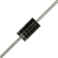
DO-201AD BYT03-400
DESCRIPTION The BYT03-400 which is using ST’s 400V planar technology, is specially suited for switching mode base drive & transistor circuits. The device, which is available in axial (DO-201AD) package, is also intended for use as a free wheeling diode in power supplies and other power switching applications.
ABSOLUTE RATINGS (limiting values) Symbol VRRM IF (AV) IFSM Tstg Tj Parameter Repetive peak reverse voltage Average forward current Surge non repetitive forward current Storage temperature range Maximum operating junction temperature TI = 55°C δ = 0.5 Value 400 3 60 - 65 to +150 150 Unit V A A °C °C
tp = 10ms Sinusoidal
October 2001 - Ed: 2A
1/5
�BYT03-400
THERMAL PARAMETERS Symbol Rth(j-a) Junction to ambient* Parameter Value 20 Unit °C/W
* On infinite heatsink with 10mm lead length.
STATIC ELECTRICAL CHARACTERISTICS Symbol IR* Parameters Reverse leakage current Test Conditions Tj = 25°C Tj = 100°C VF** Forward voltage drop Tj = 25°C Tj = 100°C Pulse test: * tp = 5ms, δ < 2% ** tp = 380µs, δ < 2% To evaluate the maximum conduction losses use the following equation: P = 1.1 x IF(AV) + 0.08 IF2(RMS) IF = 3A 1.0 VR = VRRM 0.2 Min. Typ. Max. 20 0.5 1.5 1.4 Unit µA mA V
DYNAMIC ELECTRICAL CHARACTERISTICS Symbol trr Parameter Reverse recovery time Tj = 25°C Test Conditions IF = 0.5A IR = 1A Irr = 0.25A IF = 1A dIF/dt = - 15A/µs VR = 30V tfr Forward recovery time Forward recovery voltage Tj = 25°C Tj = 25°C IF = 3A dIF/dt = 50A/µs VFR = 1.1 x VFmax IF = 3A dIF/dt = 50A/µs 75 Min. Typ. 16 Max. 25 Unit ns
55
ns
VFP
7.0
V
2/5
�BYT03-400
Fig. 1: Average forward power dissipation versus average forward current.
PF(av)(W)
5.0 4.5 4.0 3.5 3.0 2.5 2.0 1.5 1.0 0.5 0.0 0.0 0.5 1.0 1.5 2.0 2.5
T
Fig. 2: Average forward current versus ambient temperature (δ = 0.5)
IF(av)(A)
3.5
Rth(j-a)=Rth(j-l)
δ = 0.05
δ = 0.1
δ = 0.2
δ = 0.5
3.0
δ=1
2.5 2.0 1.5 1.0
Rth(j-a)=75°C/W
0.5
IF(av)(A)
δ=tp/T
3.0
tp
Tamb(°C)
0.0
3.5
0
25
50
75
100
125
150
Fig. 3: Thermal resistance versus lead length.
Fig. 4: Relative variation of thermal impedance junction ambient versus pulse duration (printed circuit board epoxy FR4, Lleads = 10mm).
Zth(j-a)/Rth(j-a)
1.0 0.9 0.8 0.7 0.6 0.5 0.4
δ = 0.5
Rth(°C/W)
90 80 70 60 50 40 30 20 10 0 5 10 15 20 25
Rth(j-l) Rth(j-a)
0.3 0.2
δ = 0.2 δ = 0.1 Single pulse
T
Lleads(mm)
0.1 0.0
tp(s)
1.E+00 1.E+01
δ=tp/T
1.E+02
tp
1.E-01
1.E+03
Fig. 5: Forward voltage drop versus forward current.
Fig. 6: Junction capacitance versus reverse voltage applied (typical values).
C(pF)
20 18
F=1MHz Vosc=30mV Tj=25°C
IFM(A)
100.0
Tj=100°C (Typical values)
16 14 12
10.0
Tj=100°C (Maximum values)
10 8
1.0
Tj=25°C (Maximum values)
6 4 2 0 1 10 100 1000
VFM(V)
0.1 0.00 0.25 0.50 0.75 1.00 1.25 1.50 1.75 2.00 2.25 2.50 2.75 3.00
VR(V)
3/5
�BYT03-400
Fig. 7: Forward recovery time versus dIF/dt (90% confidence).
tfr(ns)
200 180 160 140 120 100 80 60 40 20 0 0 10 20 30 40 50 60 70 80 90 100
IF=3A Tj=100°C
Fig. 8. Transient peak forward voltage versus dIF/dt (90% confidence).
VFP(V)
12
IF=3A Tj=100°C
10
8
6
4
2
dIF/dt(A/µs)
0 0 10 20 30
dIF/dt(A/µs)
40 50 60 70 80 90 100
Fig. 9: Peak reverse recovery current versus dIF/dt (90% confidence).
IRM(A)
2.5
IF=3A VR=200V
Fig. 10: Dynamic parameters versus junction temperature.
%
300
IF=3A dIF/dt=-50A/µs VR=30V Qrr
2.0
250
1.5
Tj=100°C
200
trr
1.0
0.5
Tj=25°C
150
IRM
dIF/dt(A/µs)
0.0 1 10 100
Tj(°C)
100 25 50 75 100 125 150
Fig. 11: Non repetitive surge peak current versus number of cycles.
IFSM(A)
65 60 55 50 45 40 35 30 25 20 15 10 5 0 1 10 100 1000
Tj initial=25°C
Number of cycles
4/5
�BYT03-400
PACKAGE MECHANICAL DATA DO-201AD
B A B ØC
note 1
E
E
note 1
ØD
ØD
note 2
DIMENSIONS REF.
A B C D E 25.40 5.30 1.30 1.25
Millimeters Min. Max.
9.50
Inches Min.
1.000 0.209 0.051 0.049
NOTES 1 - The lead diameter ∅ D is not controlled over zone E 2 - The minimum length which must stay straight between the right angles after bending is 0.59"(15 mm)
Max.
0.374
Ordering code BYT03-400 BYT03-400RL
s
Marking BYT03-400 BYT03-400
Package DO-201AD DO-201AD
Weight 1.16 g 1.16 g
Base qty 600 1900
Delivery mode Ammopack Tape & Reel
s
s
Cooling method: by conduction (method A) Epoxy meets UL 94,V0 Bending method: Application note AN1471.
Information furnished is believed to be accurate and reliable. However, STMicroelectronics assumes no responsibility for the consequences of use of such information nor for any infringement of patents or other rights of third parties which may result from its use. No license is granted by implication or otherwise under any patent or patent rights of STMicroelectronics. Specifications mentioned in this publication are subject to change without notice. This publication supersedes and replaces all information previously supplied. STMicroelectronics products are not authorized for use as critical components in life support devices or systems without express written approval of STMicroelectronics.
The ST logo is a registered trademark of STMicroelectronics © 2001 STMicroelectronics - Printed in Italy - All rights reserved. STMicroelectronics GROUP OF COMPANIES Australia - Brazil - Canada - China - Finland - France - Germany Hong Kong - India - Israel - Italy - Japan - Malaysia -Malta - Morocco - Singapore Spain - Sweden - Switzerland - United Kingdom - United States. http://www.st.com 5/5
�
很抱歉,暂时无法提供与“BYT03-400”相匹配的价格&库存,您可以联系我们找货
免费人工找货- 国内价格 香港价格
- 3600+2.006783600+0.25963
- 4200+1.969674200+0.25483
- 6000+1.889156000+0.24441
- 15000+1.7123915000+0.22155
- 30000+1.6524830000+0.21380