BYW100-200
®
HIGH EFFICIENCY FAST RECOVERY RECTIFIER DIODE
MAIN PRODUCT CHARACTERISTICS
IF(AV)
1.5 A
VRRM
200 V
Tj (max)
150 °C
VF (max)
0.85 V
FEATURES AND BENEFITS
Very low conduction losses
Negligible switching losses
Low forward and reverse recovery times
The specifications and curves enable the
determination of trr and IRM at 100°C under
users conditions.
■
■
■
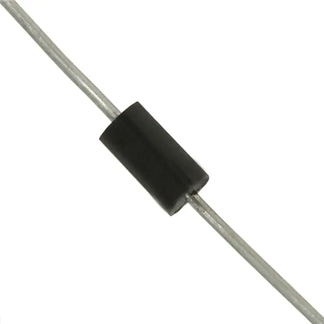
DO-15
BYW100-200
■
DESCRIPTION
Low voltage drop and rectifier suited for switching
mode base drive and transistor circuits.
ABSOLUTE RATINGS (limiting values)
Symbol
VRRM
Parameter
Value
200
Unit
V
Repetitive peak reverse voltage
IFRM
Repetitive peak forward current *
tp = 5µs F = 1KHz
80
A
IF(AV)
Average forward current*
Ta = 95°C δ = 0.5
1.5
A
IFSM
Surge non repetitive forward current
tp=10 ms Sinusoidal
50
A
Tstg
Storage temperature range
-65 +150
°C
+ 150
°C
230
°C
Tj
Maximum operating junction temperature
TL
Maximum lead temperature for soldering during 10s at 4mm from
case
* On infinitive heatsink with 10mm lead length
October 2001 - Ed: 4B
1/5
�BYW100-200
THERMAL RESISTANCES
Symbol
Rth (j-a)
Parameter
Junction to ambient*
Value
Unit
45
°C/W
* On infinite heatsink with 10mm lead length.
STATIC ELECTRICAL CHARACTERISTICS
Symbol
Parameter
Tests conditions
IR *
Reverse leakage current
Tj = 25°C
Min.
Typ.
VR = VRRM
Tj = 100°C
VF **
Forward voltage drop
Tj = 25°C
IF = 4.5A
Tj = 100°C
IF = 1.5A
0.78
Max.
Unit
10
µA
0.5
mA
1.2
V
0.85
Pulse test : * tp = 5 ms, δ < 2 %
** tp = 380 µs, δ < 2 %
To evaluate the maximum conduction losses use the following equation :
P = 0.75 x IF(AV) + 0.075 x IF2(RMS)
RECOVERY CHARACTERISTICS
Symbol
2/5
Tests conditions
Min.
Typ.
Max.
Unit
35
ns
trr
IF = 1A dIF/dt = - 50A/µs VR = 30V
Tj = 25°C
tfr
IF = 1.5A dIF/dt = - 50A/µs
Measured at 1.1 x VFmax
Tj = 25°C
30
ns
VFP
IF = 1.5A dIF/dt = - 50A/µs
Tj = 25°C
5
V
Qrr
IF = 1.5A dIF/dt = - 20A/µs VR ≤ 30V
Tj = 25°C
10
nC
�BYW100-200
Fig. 1: Average forward power dissipation versus
average forward current.
PF(av)(W)
1.6
δ = 0.05
δ = 0.1
δ = 0.2
δ=1
δ = 0.5
1.4
1.2
1.0
0.8
0.6
T
0.4
0.2
0.0
0.0
δ=tp/T
IF(av) (A)
0.2
0.4
0.6
0.8
1.0
1.2
1.4
tp
1.6
1.8
Fig. 2: Average forward current versus ambient
temperature (δ=0.5).
1.8
1.6
1.4
1.2
1.0
0.8
0.6
0.4
0.2
0.0
IF(av)(A)
Rth(j-a)=Rth(j-l)
Rth(j-a)=100°C/W
Tamb(°C)
0
50
75
100
125
150
Fig. 4: Variation of thermal impedance junction to
ambient versus pulse duration (recommended pad
layout, epoxy FR4, e(Cu) = 35µm).
Fig. 3: Thermal resistance versus lead length.
Rth(°C/W)
110
100
90
80
70
60
50
40
30
20
10
0
25
Zth(j-a)/Rth(j-a)
1.00
Rth(j-a)
δ = 0.5
δ = 0.2
Rth(j-l)
0.10
δ = 0.1
Single pulse
Lleads(mm)
5
10
15
20
25
Fig. 5: Forward voltage drop versus forward
current (maximum values).
50.00
0.01
1E-2
1E-1
tp(s)
1E+0
1E+1
1E+2
5E+2
Fig. 6: Junction capacitance versus reverse
voltage applied (typical values).
IFM(A)
20
C(pF)
F=1MHz
Tj=25°C
Tj=100°C
(Typical values)
10
10.00
Tj=25°C
5
Tj=100°C
1.00
2
VFM(V)
0.10
0.0 0.2 0.4 0.6 0.8 1.0 1.2 1.4 1.6 1.8 2.0 2.2 2.4 2.6
VR(V)
1
1
10
100
200
3/5
�BYW100-200
Fig. 7: Reverse recovery time versus dIF/dt.
150
Fig. 8: Peak reverse recovery current versus
dIF/dt.
trr(ns)
2.5
IF=1.5A
VR=30V
90% confidence
Tj=100°C
IRM(A)
IF=1.5A
VR=30V
90% confidence
2.0
100
1.5
Tj=100°C
Tj=25°C
1.0
50
Tj=25°C
0.5
0
dIF/dt(A/µs)
1
10
100
Fig. 9: Dynamic parameters versus junction
temperature.
250
%
Qrr
200
IRM
150
100
25
4/5
trr
50
75
Tj(°C)
100
125
0.0
dIF/dt(A/µs)
1
10
100
�BYW100-200
PACKAGE MECHANICAL DATA
DO-15
DIMENSIONS
C
D
■
■
REF.
C
A
B
Millimeters
Inches
Min.
Max.
Min.
Max.
A
6.05
6.75
0.238
0.266
B
2.95
3.53
0.116
0.139
C
26
31
1.024
1.220
D
0.71
0.88
0.028
0.035
Ordering code
Marking
Package
Weight
Base qty
Delivery mode
BYW100-200
BYW100-200
DO-15
0.4 g
1000
Ammopack
BYW100-200RL
BYW100-200
DO-15
0.4 g
6000
Tape and reel
White band indicates cathode
Epoxy meets UL 94,V0
Information furnished is believed to be accurate and reliable. However, STMicroelectronics assumes no responsibility for the consequences of
use of such information nor for any infringement of patents or other rights of third parties which may result from its use. No license is granted by
implication or otherwise under any patent or patent rights of STMicroelectronics. Specifications mentioned in this publication are subject to
change without notice. This publication supersedes and replaces all information previously supplied.
STMicroelectronics products are not authorized for use as critical components in life support devices or systems without express written approval of STMicroelectronics.
The ST logo is a registered trademark of STMicroelectronics
© 2001 STMicroelectronics - Printed in Italy - All rights reserved.
STMicroelectronics GROUP OF COMPANIES
Australia - Brazil - Canada - China - Finland - France - Germany
Hong Kong - India - Israel - Italy - Japan - Malaysia -Malta - Morocco - Singapore
Spain - Sweden - Switzerland - United Kingdom - United States.
http://www.st.com
5/5
�
很抱歉,暂时无法提供与“BYW100-200RL”相匹配的价格&库存,您可以联系我们找货
免费人工找货