物料型号:CS70
器件简介:CS70是一款用于测量高侧分流电阻上的微小差分电压,并将其转换为地参考输出电压的器件。它具有可调节的增益,范围从20 V/V到100 V/V,并且具有宽输入共模电压范围和低静态电流。
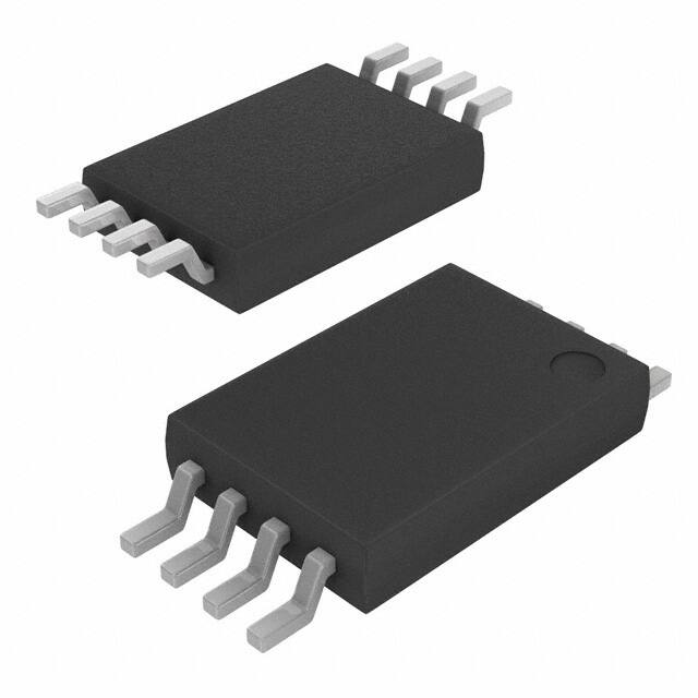
引脚分配:CS70采用TSSOP8封装,具有8个引脚,包括模拟输出(Out)、电源地(Gnd)、正电源(Vcc+)、负电源(Vcc-)、模拟输入(Vp, Vm)、增益选择引脚(SEL1, SEL2)。
参数特性:
- 独立的供电和输入共模电压
- 宽共模工作范围:单电源配置下2.9 V至70 V,双电源配置下-2.1 V至65 V
- 低电流消耗:最大360 µA
- 增益可选:20 V/V, 25 V/V, 50 V/V 或 100 V/V
- 缓冲输出
功能详解:CS70可以用于无线电池充电器、便携设备充电器、精密电流源和可穿戴设备等应用。它能够在待机模式下将输入漏电流降至几乎为零,从而最小化功耗。
应用信息:CS70可用于测量电流,并将信息反馈给微控制器。
封装信息:CS70采用TSSOP8塑料封装,具有紧凑的尺寸和良好的热性能。