DK3300-ELCD
DK3300-ELCD Development Kit
DATA BRIEFING
FEATURES SUMMARY
■
CONTAINS ALL THE ITEMS NEEDED TO
EXPLORE THE TURBO uPSD3300 MCU:
– DK3300-ELCD Development Board
(populated with the uPSD3334D and
enhanced graphic LCD)
– Keil ULINK USB-JTAG Adapter
– Raisonance R-LINK-ST USB-JTAG
Adapter
– Raisonance RKIT CD
– RS-232 Cable and USB Cables
– 110/220V Universal Power Supply
– DK3300-ELCD ST CD
– Quick Start Guide
AVAILABLE FOR ONLINE ORDERING
SUPPORTS 3rd PARTY DEVELOPMENT
TOOLS
Figure 1. Development Kit Contents
)
s
(
t
c
u
d
o
)
r
s
(
P
t
c
e
t
u
e
d
l
o
o
r
s
P
b
e
O
t
e
l
)
o
s
(
s
t
b
c
u
O
d
o
)
r
s
P
(
t
c
e
t
u
e
l
d
o
o
r
s
P
b
O
e
t
e
l
o
s
b
O
■
■
Table 1. Ordering Information
Part Number
Voltage
Price (in US$)
DK3300(1,2)
Universal (100V - 240V)
199.00
DK3300-ELCD
Universal (100V - 240V)
199.00
Note: 1. NND =Not for New Design
2. This product is still valid; it just has the regular LCD. Schematics and sample code for this kit is available at www.st.com/psm/.
December 2004
For further information contact your local ST sales office.
1/13
�DK3300-ELCD - DEVELOPMENT KIT
TABLE OF CONTENTS
FEATURES SUMMARY . . . . . . . . . . . . . . . . . . . . . . . . . . . . . . . . . . . . . . . . . . . . . . . . . . . . . . . . . . . . . 1
Figure 1. Development Kit Contents . . . . . . . . . . . . . . . . . . . . . . . . . . . . . . . . . . . . . . . . . . . . . . . . . 1
Table 1. Ordering Information . . . . . . . . . . . . . . . . . . . . . . . . . . . . . . . . . . . . . . . . . . . . . . . . . . . . . 1
SUMMARY DESCRIPTION . . . . . . . . . . . . . . . . . . . . . . . . . . . . . . . . . . . . . . . . . . . . . . . . . . . . . . . . . . . 3
DK3300-ELCD CD Contents . . . . . . . . . . . . . . . . . . . . . . . . . . . . . . . . . . . . . . . . . . . . . . . . .
Raisonance CD Contents . . . . . . . . . . . . . . . . . . . . . . . . . . . . . . . . . . . . . . . . . . . . . . . . . . .
DK3300-ELCD demonstrations . . . . . . . . . . . . . . . . . . . . . . . . . . . . . . . . . . . . . . . . . . . . . .
Documentation . . . . . . . . . . . . . . . . . . . . . . . . . . . . . . . . . . . . . . . . . . . . . . . . . . . . . . . . . . .
3rd Party Development Tools. . . . . . . . . . . . . . . . . . . . . . . . . . . . . . . . . . . . . . . . . . . . . . . .
Table 2. Additional Resources for DK3300-ELCD Components . . . . . . . . . . . . . . . . . . . . . .
.....3
.....3
.....3
.....3
.....3
.....3
)
s
(
t
c
u
d
o
)
r
s
(
P
t
c
e
t
u
e
d
l
o
o
r
s
P
b
e
O
t
e
l
)
o
s
(
s
t
b
c
u
O
d
o
)
r
s
P
(
t
c
e
t
u
e
l
d
o
o
r
s
P
b
O
e
t
e
l
o
s
b
O
PART NUMBERING . . . . . . . . . . . . . . . . . . . . . . . . . . . . . . . . . . . . . . . . . . . . . . . . . . . . . . . . . . . . . . . . 4
Table 3. Ordering Information Scheme . . . . . . . . . . . . . . . . . . . . . . . . . . . . . . . . . . . . . . . . . . . . . . 4
APPENDIX A.DK3300-ELCD SCHEMATICS . . . . . . . . . . . . . . . . . . . . . . . . . . . . . . . . . . . . . . . . . . . . . 5
Figure 2.
Figure 3.
Figure 4.
Figure 5.
Figure 6.
Top Level . . . . . . . . . . . . . . . . . . . . . . . . . . . . . . . . . . . . . . . . . . . . . . . . . . . . . . . . . . . . . . 5
MCU. . . . . . . . . . . . . . . . . . . . . . . . . . . . . . . . . . . . . . . . . . . . . . . . . . . . . . . . . . . . . . . . . . 6
Power. . . . . . . . . . . . . . . . . . . . . . . . . . . . . . . . . . . . . . . . . . . . . . . . . . . . . . . . . . . . . . . . . 7
Peripherals. . . . . . . . . . . . . . . . . . . . . . . . . . . . . . . . . . . . . . . . . . . . . . . . . . . . . . . . . . . . . 8
Connectors . . . . . . . . . . . . . . . . . . . . . . . . . . . . . . . . . . . . . . . . . . . . . . . . . . . . . . . . . . . . 9
APPENDIX B.DK3300-ELCD Board . . . . . . . . . . . . . . . . . . . . . . . . . . . . . . . . . . . . . . . . . . . . . . . . . . 10
Figure 7. DK3300-ELCD Board Connections . . . . . . . . . . . . . . . . . . . . . . . . . . . . . . . . . . . . . . . . . 10
APPENDIX C.DK3300-ELCD JUMPERS . . . . . . . . . . . . . . . . . . . . . . . . . . . . . . . . . . . . . . . . . . . . . . . 11
Table 4. DK3300-ELCD Jumpers Selection and Defaults . . . . . . . . . . . . . . . . . . . . . . . . . . . . . . . 11
REVISION HISTORY. . . . . . . . . . . . . . . . . . . . . . . . . . . . . . . . . . . . . . . . . . . . . . . . . . . . . . . . . . . . . . . 12
Table 5. Document Revision History . . . . . . . . . . . . . . . . . . . . . . . . . . . . . . . . . . . . . . . . . . . . . . . 12
2/13
�DK3300-ELCD - DEVELOPMENT KIT
SUMMARY DESCRIPTION
The DK3300-ELCD is a development kit for the
uPSD3300 family (see Table 2) which is a series
of 8051 class microcontrollers (MCUs) that contain
a fast Turbo 8032 core with a large Dual Bank
Flash memory, a large SRAM, many peripherals,
programmable logic, and a JTAG Debug/In System Programming (ISP) port.
DK3300-ELCD CD Contents
Featured applications include those listed below
for third-party development, however, the uPSD is
compatible with any compiler supporting standard
8051 architecture.
– Keil uVision2: code-size-limited version
Raisonance CD Contents
– PSDsoft Express
– Raisonance Rkit Development Suite: codesize-limited version
– Includes full-featured debugger (unlimited)
DK3300-ELCD demonstrations
– Example code file (1) – BANKING.zip
– Example code file (2) – EEPROM_EMUL.zip
– Example code file (3) – I2C.zip
– Example code file (4) –
NEW_DK3300_PROJECT.zip
– Device drivers for PWM, I2C, and so forth dk33_dd.zip
– PWM example code - PWM_ADC.zip
– SPI example code – SPI.zip
Documentation
– DK3300-ELCD User Manual (Quick Start
Guide)
3rd Party Development Tools
– Keil uVision2 (Integrated Development
Environment)
– ULINK USB-JTAG Adapter
– Raisonance Rkit Development Suite
– R-LINK-ST USB-JTAG Adapter
)
s
(
t
c
u
d
o
)
r
s
(
P
t
c
e
t
u
e
d
l
o
o
r
s
P
b
e
O
t
e
l
)
o
s
(
s
t
b
c
u
O
d
o
)
r
s
P
(
t
c
e
t
u
e
l
d
o
o
r
s
P
b
O
e
t
e
l
o
s
b
O
Table 2. Additional Resources for DK3300-ELCD Components
Component
Link
uPSD3300 Product web page
http://www.st.com/stonline/products/families/memories/psm/
upsd3300.htm
DK3300-ELCD Quick Start Guide
http://www.st.com/stonline/books/pdf/docs/10394.pdf
PSDsoft Express
http://www.st.com/stonline/products/families/memories/psm/
soft_c2.htm
DK3300-ELCD Development Board (schematics)(1) http://psmdev.st.com/DK3300-ELCD_schematics.zip
uPSD3334D (populates the DK3300-ELCD
Development Board)
http://www.st.com/stonline/products/families/memories/psm/
upsd33tb.htm
Keil ULINK USB-JTAG Adapter
http://www.keil.com/c51/
Raisonance R-LINK-ST USB-JTAG Adapter
http://www.raisonance.com/
Banking Example Code(1)
http://www.st.com/stonline/products/families/memories/psm/
support/BANKING.zip
EEPROM Emulation Example Code(1)
http://www.st.com/stonline/products/families/memories/psm/
support/EEPROM_EMUL.zip
I2C Example Code(1)
http://www.st.com/stonline/products/families/memories/psm/
support/I2C.zip
New DK3300 project Example Code(1)
http://www.st.com/stonline/products/families/memories/psm/
support/NEW_DK3300_PROJECT.zip
Device Drivers(1)
http://www.st.com/stonline/products/families/memories/psm/
support/dk33_dd.zip
PWM Example Code(1)
http://www.st.com/stonline/products/families/memories/psm/
support/PWM_ADC.zip
SPI Example Code(1)
http://www.st.com/stonline/products/families/memories/psm/
support/SPI.zip
Note: 1. This product is still valid; it just has the regular LCD. Schematics and sample code for this kit is available at www.st.com/psm/.
3/13
�DK3300-ELCD - DEVELOPMENT KIT
PART NUMBERING
Table 3. Ordering Information Scheme
Example:
DK
33
0
0
–
ELCD
Part Type
DK = Development Kit
Family
)
s
(
t
c
u
d
o
)
r
s
(
P
t
c
e
t
u
e
d
l
o
o
r
s
P
b
e
O
t
e
l
)
o
s
(
s
t
b
c
u
O
d
o
)
r
s
P
(
t
c
e
t
u
e
l
d
o
o
r
s
P
b
O
e
t
e
l
o
s
b
O
33 = uPSD 33XX Turbo core
Power Type
0 = Self-powered
On-chip Flash Memory Size
0 = 288KB Flash
LCD Type
blank = Regular LCD (NND - Not for New Design)(1)
ELCD = Enhanced graphic LCD
Note: 1. This product is still valid; it just has the regular LCD. Schematics and sample code for this kit is available at www.st.com/psm/.
4/13
�D
C
B
A
1
1
2
Power
(Input/Output)
3
CPU_PB Port Usage:
PB[0] - 41ST87
PB[7:5] - Encoder
PB[4:1] - LCD
MCU
Top Level DK3300-ELCD
3
Peripherals
4
Connector
4
5
5
Number
4-November-2004
Date:
File:
Top Level DK3300-ELCD
Size
B
Title
)
s
(
t
c
u
d
o
)
r
s
(
P
t
c
e
t
u
e
d
l
o
o
r
s
P
b
e
O
t
e
l
)
o
s
(
s
t
b
c
u
O
d
o
)
r
s
P
(
t
c
e
t
u
e
l
d
o
o
r
s
P
b
O
e
t
e
l
o
s
b
O
2
6
6
Revision
D
C
B
A
DK3300-ELCD - DEVELOPMENT KIT
APPENDIX A. DK3300-ELCD SCHEMATICS
Figure 2. Top Level
AI10465
5/13
�D
C
B
A
CSTCW-X
2
X1
1
GND
CPU_UART2
CPU_ADC_IN
CPU_I2C
CPU_P3
CPU_CMM
1
2
JP1
CPU Reset
CPU_CLOCK
1
CPU_SPI_BUS
CPU_PWM_OUT
3
X2
6
4
2
JP11
C36
49
X2
CPU_PWM0
CPU_PWM1
CPU_PWM2
CPU_PCA0CLK
CPU_SPI_CLK
CPU_SPI_RXD
CPU_SPI_TXD
CPU_SPI_SEL
A3.3V
GND
CPU_ADC0
CPU_ADC1
CPU_U2RXD
CPU_U2TXD
CPU_ADC4
CPU_ADC5
CPU_ADC6
CPU_ADC7
VREF
CPU_U1RXD
CPU_U1TXD
CPU_INT0
CPU_INT1
CPU_P3.4
CPU_P3.5
CPU_I2CSDA
CPU_I2CSCL
33
31
30
27
25
23
19
18
70
72
69
52
54
56
58
59
60
61
64
75
77
79
2
40
42
44
46
8
CPU_RST 68
48
X1
20pF
C18
X2
40MHz
103P
CPU_DEBUG
JTAG_CNTRL
5
3
1
X1
PA0
PA1
PA2
PA3
PA4
PA5
PA6
PA7
CTRL0/WR
CTRL0/RD
CTRL2/PSEN
ALE(PD0)
P2.0/A8
P2.1/A9
P2.2/A10
P2.3/A11
P0.0/AD0
P0.1/AD1
P0.2/AD2
P0.3/AD3
P0.4/AD4
P0.5/AD5
P0.6/AD6
P0.7/AD7
2
3.3V
5V
PD1
PD2
ADC0/T2/P1.0
ADC1/T2x/P1.1.
ADC2/RXD2/P1.2
ADC3/TXD2/P1.3
ADC4/SPISCLK/P1.4
ADC5/SPIRXD/P1.5
PB0
ADC6/SPITXD/P1.6
PB1
ADC7/SPISEL/P1.7
PB2
PB3
VREF
PB4
AVCC
PB5
PB6
AGND + PSDGND
PB7
T2/TCM0/P4.0
T2x/TCM1/P4.1
TMS/PC0
RXD2/TCM2/P4.2
TCK/PC1
TXD2/PCA0/P4.3
VSTBY/PC2
SPISCLK/TCM3/P4.4
TSTAT/RDY/PC3
SPIRXD/TCM4/P4.5 TERR/V
BATON/PC4
SPITXD/TCM5/P4.6
TDI/PC5
SPISEL/PCA1/P4.7
TDO/PC6
PC7
RXD/P3.0
TXD/P3.1
EXINT0/GATE0/P3.2
EXINT1/GATE1/P3.3
T0/P3.4
T1/P3.5
I2CSDA/P3.6
I2CSCL/P3.7
DEBUG
RESET_IN
X2
X1
U3
uPSD3334D-80
3 CPU_PD1
1 CPU_PD2
20 CPU_TMS
16 CPU_TCK
15 CPU_PC2
14 CPU_TSTA
9 CPU_TERR
7 CPU_TDI
6 CPU_TDO
5 CPU_PC7
80 CPU_PB0
78 CPU_PB1
76 CPU_PB2
74 CPU_PB3
73 CPU_PB4
71 CPU_PB5
67 CPU_PB6
66 CPU_PB7
35 CPU_PA0
34 CPU_PA1
32 CPU_PA2
28 CPU_PA3
26 CPU_PA4
24 CPU_PA5
22 CPU_PA6
21 CPU_PA7
62 CPU_WR
65 CPU_RD
63 CPU_PSEN
4 CPU_ALE
51 CPU_AD8
53 CPU_AD9
55 CPU_AD10
57 CPU_AD11
36 CPU_AD0
37 CPU_AD1
38 CPU_AD2
39 CPU_AD3
41 CPU_AD4
43 CPU_AD5
45 CPU_AD6
47 CPU_AD7
3
3
CPU_JTAG
PB[0.. 7]
PA[0.. 7]
Control Bus
AD[8.. 11]
AD[0.. 7]
MCU
VREF
5V
5V
C14
22µ
C16
104P
C11
104P
100µH
L3
C15
22µ
3.3V
JTAG (FlashLINK)
C12
104P
AVCC
C43
104P
A3.3V
CPU_TMS
CPU_TCK
CPU_TSTA
CPU_TERR
CPU_TDI
CPU_TDO
JTAG_CTRL
CPU_RST
CPU_DEBUG
4
C10 and C7 are
22µ B-size, Tantalum capacitors.
C10
22µ
3.3V
C42
22µ
3.3V low active RESET
CPU_JTAG
4
5
6
7
8
R1
10K
5
14
12
10
8
6
4
2
TDO
TCK
TMS
VCC
TDI
GND
JEN
JTAG
TERR
GND
GND
RST
TSTAT
CNTL
TRST
13
11
9
7
5
3
1
6
5
Date:
File:
Size
B
Title
R6
10K
4-November-2004
Number
MCU
C4
105P
RC_RST
D3
1N4148
3.3V
Reset Circuit
RESET
CPU_RST
3
2
1
6
JP8
FlashLINK JTAG for 3300 Programming/Debugging
R4
470
D1
RED
R2
10K
5V
5V
RESET
SWITCH
PUSH-BUTTON
Reset
4
3
2
1
C17
VCC
VDD
VDD
10
12
50
8
7
6
5
1
2
3
4
20pF
GND
GND
GND
13
29
3
5
Clock
N.C.
N.C.
11
17
2
1
6/13
4
2
)
s
(
t
c
u
d
o
)
r
s
(
P
t
c
e
t
u
e
d
l
o
o
r
s
P
b
e
O
t
e
l
)
o
s
(
s
t
b
c
u
O
d
o
)
r
s
P
(
t
c
e
t
u
e
l
d
o
o
r
s
P
b
O
e
t
e
l
o
s
b
O
1
5V
Revision
C5
104P
D
C
B
A
DK3300-ELCD - DEVELOPMENT KIT
Figure 3. MCU
AI10465
�D
C
R7
47K
5V
R8
47K
5V
CPU_PB5
CPU_PB6
CPU_PB7
Data
NI
GND
+5V
CLK
NI
5
3
1
1
CPU_INT0
CPU_INT1
PS2_DIN6_F
1
2
3
4
5
6
PS2
6
4
2
JP5
C2
104P
47Ω
R13
47Ω
R14
CPU_PD2
CPU_PD1
5V
C1
104P
R5
R3
2
4
JP6
10K
10K
2
1
3
LED-1
LED-2
3
2
1
3
4
R30 R31 R9
4K7 4K7 4K7
5V
2
1
6
5
5
4
KEY1 SW
PUSH-BUTTON
ENCODER
3
2
1
4
Power Supply
RS232, IrDA
RS232_TXD0
RS232_RXD0
CPU_COMM
KEY2 SW
PUSH-BUTTON
3
Encoder, Button, & LED
7
B
3
4
4
2
3
1
J1
RXD1
TXD1
1
5
2
6
4
5V
C34
4.7µF
3.3V
SW2-SPDT
3
CPU_U1TXD
JP16
4
CPU_U1RXD
CPU_U1RXD
CPU_U1TXD
4
3.3V
3
SW1
VIN
VOUT
2
C40
100µF
1N4004
D2
1N4004
1N4004
D7
D6
GND
C28
10µF
3.3V
5
Size
B
C27
104pF Date:
File:
Title
1 V
IN
C21
334pF
15
C29
10µF
100µF
4-November-2004
Number
Input/Output
6
5V
6
C26
104pF
TXD1
RXD1
UART1
UART0
Revision
D4
POWER
R17
1K
1
6
2
7
3
8
4
9
5
1
6
RS232_TXD0 2
7
RS232_RXD0 3
8
4
9
5
C39
TXD1
RXD1
7
8
13 RS232_RXD0
14 RS232_TXD0
4
5
16
VOUT 3
U6
78M05-5V
TFDU4300
GND
VLOGIC
VCC1
Cathode
Annode (VCC2)
SD
RXD
TXD
C30
220µF
VUNREG
8
7
U5
LD1117-3.3V
D5
1N4004
2
5
C37
0.1µF
1
R19
5
4
3
47k
C38
4.7µF
V–
R2OUT R2IN
T2IN T2OUT
R1OUT R1IN
T1IN T1OUT
C2+
C2–
C1+
C1–
VCC
V+
U8
3.3V
IrDA Interface Circuit (disable shutdown)
U9
6
C31
0.1µF
5
ST3232
RS232 Interface Circuit
C20
334pF
6
9
10
12
11
C22
334pF 3
1
C23
334pF 2
R20
C32
104pF
3.3V
0
10
A
2
1
3
2
1
3
GND
1
GND
2
2
)
s
(
t
c
u
d
o
)
r
s
(
P
t
c
e
t
u
e
d
l
o
o
r
s
P
b
e
O
t
e
l
)
o
s
(
s
t
b
c
u
O
d
o
)
r
s
P
(
t
c
e
t
u
e
l
d
o
o
r
s
P
b
O
e
t
e
l
o
s
b
O
1
D
C
B
A
DK3300-ELCD - DEVELOPMENT KIT
Figure 4. Power
AI10467
7/13
�D
C
B
A
5V
C35
104P
C3
104pF
3.3V
2
4
JP4
3
2
1
JP3
LCD_VL
1
1
3
1
2
3
4
LM358
OP-A
IP-A
IP_A
GND
U2
V0
LCD_E2
LCD_E1
HEADER 2x2
CPU_PB4
CPU_PB5
VCC
OP-B
IP-B
IP_B
R33
4K7
R0
4K7
3
4
CPU_RST
2
SPI_SEL
1
Q
VSS
C
D
VCC
HOLD
8
7
6
5
5V
48PE16
S
6
5
8
7
CPU_SPI_RXD
5 3.3V
6 3.3V
7 GND
8
CPU_SPI_CLK
CPU_SPI_TXD
3.3V
2
RS
R/W
E
D0
D1
D2
D3
D4
D5
D6
D7
LCD
VDD 2
3
V0
VSS 1
7
NC 5
NC
18
RST
LCD_GXM12232SL
6
8
9
4
10
11
12
13
14
15
16
17
PB[5.. 7]
LCD_E2
LCD_E1
CPU_PB2
CPU_PB1
CPU_PA0
CPU_PA1
CPU_PA2
CPU_PA3
CPU_PA4
CPU_PA5
CPU_PA6
CPU_PA7
PA[0.. 7]
5V
5V
V0
C6
104P
LCD Interface Circuit
SPI Interface Circuit
LCD Module Only Operates on 5V
W
RESET VCC
C
D
U10
W
VSS
S
Q
U4
M95080W
CPU_SPI_TXD
3
4
1
2
CPU_SPI_CLK
3.3V
CPU_SPI_SEL
SPI_SEL
CPU_SPI_RXD
C19
104P
VCC
2
1
JP7
CON3
3
2
1
CON4
2
1
CON5 5V
1
2
CON6
3
PWM, ADC
7101UART2
7101ADC
4
GND
4
C25
104pF
CPU_PWM0
CPU_ADC7
CPU_ADC6
CPU_ADC5
CPU_ADC4
CPU_U1TXD
CPU_U1RXD
CPU_ADC1
CPU_ADC0
GND
GND
10K
JP15
1
3
5
2
4
6
2
4
6
8
10
12
14
16
R18
1
3
5
7
9
11
13
15
JP14
SENSOR2
SENSOR1
R25 R27
1k2 47k
RESET
F32k
R22
4K7
R23
V_UNREG 4K7
R26
12k
5V
R24
4K7
5V
8
7
6
5
1
2
3
4
M41ST87_VOUT
C24
105pF
R21
10K
I2CSDA
I2CSCL
I2C Interface Circuit with Battery
3
20
24
23
13
10
11
17
22
27
9
5V
2
14
M41ST87_PFO 11
M41ST87_SQW 8
M41ST87_PFO 25
CPU_PB1
F32k
PFO1
PFO2
IRQ
SQW
RST
VOUT
TPCLR
ECON
5
JP12
1
2
3
4
JP18
Number
4-November-2004
1
3
6
1
2
2
4
JP9
6
JP10
CPU_PC2
M41ST87_VOUT
CPU_I2CSDA
CPU_I2CSCL
Date:
File:
Peripheral
CPU_INT1
CPU_INT0
ECON
TPCLR
F32k
GND
F32k
Size
B
Title
15
12
13
9
10
6
7
3
4
1
21
12 M41ST87_PFO1
7 M41ST87_PFO2
26 M41ST87_IRQ
8 M41ST87_SQW
19 RESET
25 M41ST87_VOUT
18 TPCLR
16 ECON
U7
3.3V or 5V
M41ST87
M41ST87_IRQ
TP1IN
TP2IN
PFI1
PFI2
RST INT1
RST INT2
SDA
SCL
EX
WDI
104pF
C33
LCD_VL
GND
5
Battery Socket
BATTERY
15
VBAT
R15
10K
2
28
VCC
VSS
8/13
14
3.3V
)
s
(
t
c
u
d
o
)
r
s
(
P
t
c
e
t
u
e
d
l
o
o
r
s
P
b
e
O
t
e
l
)
o
s
(
s
t
b
c
u
O
d
o
)
r
s
P
(
t
c
e
t
u
e
l
d
o
o
r
s
P
b
O
e
t
e
l
o
s
b
O
1
Revision
I2CSDA
I2CSCL
D
C
B
A
DK3300-ELCD - DEVELOPMENT KIT
Figure 5. Peripherals
AI10468
�D
C
B
A
1
2
2
GND
GND
CPU_PB7
CPU_PB5
CPU_PB3
CPU_PB2
CPU_PB1
CPU_PB0
CPU_PD2
GND
GND
GND
Connector
2
4
2
4
6
8
10
12
14
16
18
20
CON3
3
1
3
5
7
9
11
13
15
17
19
HEADER 2x2
1
3
CON7
3
3.3V
CPU_RST
CPU_PB6
CPU_PB4
CPU_U0RXD
CPU_U0TXD
CPU_INT0
CPU_INT1
CPU_PD1
5V
A3.3V
A3.3V
2
4
6
8
10
12
14
16
18
20
22
24
26
28
30
32
34
36
CON2
1
3
5
7
9
11
13
15
17
19
CON1
1
3
5
7
9
11
13
15
17
19
21
23
25
27
29
31
33
35
2
4
6
8
10
12
14
16
18
20
4
HEADER 18x2
GND
CPU_PA0
CPU_PA1
CPU_PA2
CPU_PA3
CPU_PA4
CPU_PA5
CPU_PA6
CPU_PA7
GND
CPU_TCK
CPU_TSTAT
CPU_DEBUG
CPU_TDO
GND
CPU_ALE
CPU_PSEN
GND
X2
CPU_AD7
CPU_AD6
CPU_AD5
CPU_AD4
CPU_AD3
CPU_AD2
CPU_AD1
CPU_AD0
GND
4
5V
CPU_PWM0
CPU_PWM1
CPU_PWM2
CPU_PCA0CLK
CPU_SPI_CLK
CPU_SPI_RXD
CPU_SPI_TXD
CPU_SPI_SEL
CPU_TMS
CPU_PC2
CPU_TERR
CPU_TDI
CPU_PC7
GND
CPU_WR
CPU_RD
3.3V
GND
CPU_I2CSCL
CPU_I2CSDA
CPU_P3.5
CPU_P3.4
CPU_A8
CPU_A9
CPU_A10
CPU_A11
3.3V
5
5
Number
4-November-2004
Date:
File:
Connector
Size
B
Title
)
s
(
t
c
u
d
o
)
r
s
(
P
t
c
e
t
u
e
d
l
o
o
r
s
P
b
e
O
t
e
l
)
o
s
(
s
t
b
c
u
O
d
o
)
r
s
P
(
t
c
e
t
u
e
l
d
o
o
r
s
P
b
O
e
t
e
l
o
s
b
O
1
6
6
Revision
D
C
B
A
DK3300-ELCD - DEVELOPMENT KIT
Figure 6. Connectors
AI10469
9/13
�DK3300-ELCD - DEVELOPMENT KIT
APPENDIX B. DK3300-ELCD BOARD
Figure 7. DK3300-ELCD Board Connections
)
s
(
t
c
u
d
o
)
r
s
(
P
t
c
e
t
u
e
d
l
o
o
r
s
P
b
e
O
t
e
l
)
o
s
(
s
t
b
c
u
O
d
o
)
r
s
P
(
t
c
e
t
u
e
l
d
o
o
r
s
P
b
O
e
t
e
l
o
s
b
O
10/13
�DK3300-ELCD - DEVELOPMENT KIT
APPENDIX C. DK3300-ELCD JUMPERS
The following Table describes the DK3300-ELCD
Jumpers. Verify that in Jumper set JP14 – ADC7
is “closed” and JP3 is set to “Fix.” JP5, JP4 and
JP6 Jumper sets are all “closed” for the PWMADC
demonstration.
See the Schematics (Figure 3., page 6, Figure
4., page 7, Figure 5., page 8, and Figure
6., page 9) for more information regarding the
jumpers.
Table 4. DK3300-ELCD Jumpers Selection and Defaults
Jumper
Number
JP1
Description
JTAGDebug I/O Pin
Default Settings
Closed
Comments
Should be Closed
)
s
(
t
c
u
d
o
)
r
s
(
P
t
c
e
t
u
e
d
l
o
o
r
s
P
b
e
O
t
e
l
)
o
s
(
s
t
b
c
u
O
d
o
)
r
s
P
(
t
c
e
t
u
e
l
d
o
o
r
s
P
b
O
e
t
e
l
o
s
b
O
JP2
Reset Input Select
Closed in position 1-2 for Reset
Switch
Position 2-3 for RTC Reset
JP3
LCD Contrast
2-3 Closed (Fix)
Normally Closed in position 2-3; Position 1-2
used for PWM Control
JP4
Enhanced LCD
Closed
Determines if Enhanced-LCD in On-Board
JP5
Encoder Connection
Normally all 3 Closed to enable
Encoder
This connects Encoder to Port B.
JP6
Key board and LED
Closed
JP7
Enable SPI
Closed
Normally closed to enable SPI EEPROM
JP8
IrDA/UART1 Select
Normally 1-3 and 2-4; Closed to
select the RS232 Connector 1
Else can be set to position 3-5 and 4-6 to select
the IrDA transceiver to be connected to UART1
JP9
SRAM Battery
Normally Open
JP10
Enable I2C
Closed
Normally both positions closed to enable I2C
access to RTC chip.
JP11
Clock Select
Closed x2 for Crystal
Selects Crystal or Oscillator
JP12
Interrupt Select
(for MCU)
Normally Open (See DK3300ELCD SCHEMATICS)
(Used to map various RTC Interrupt sources to
the MCU) 1-IRQ; 2-PFO2; 3-SQW; 4-PFO1;
and 5-PBO
JP14
ADC Channel Select
ADC7 ( Positions 15-16) is
Closed
ADC7 ( Positions 15-16) is Closed
JP15
PWM RC Constant
Normally (position 1-2) is
Closed
Selects PWM RC constant; position 1-2 is 1ms.
JP16
For connecting
UART0 and UART1
in loop back mode
Normally Open
Can be connected positions 1-2 and 3-4 for loop
back
Normally not used
Headers can be used to connect to check
signals:
1 - ECON
2 - TPCLR
3 - F32k
4 - GND
JP18
Headers for
M41ST87 Signals
11/13
�DK3300-ELCD - DEVELOPMENT KIT
REVISION HISTORY
Table 5. Document Revision History
Date
Version
Description
31-May-04
1.0
First Edition - DK3300 (NND - Not for New Design)
09-Dec-04
2.0
New DK3300-ELCD features added (Figure 2, 3, 4, 5, 6; Table 1, 2, 3)
)
s
(
t
c
u
d
o
)
r
s
(
P
t
c
e
t
u
e
d
l
o
o
r
s
P
b
e
O
t
e
l
)
o
s
(
s
t
b
c
u
O
d
o
)
r
s
P
(
t
c
e
t
u
e
l
d
o
o
r
s
P
b
O
e
t
e
l
o
s
b
O
12/13
�DK3300-ELCD - DEVELOPMENT KIT
)
s
(
t
c
u
d
o
)
r
s
(
P
t
c
e
t
u
e
d
l
o
o
r
s
P
b
e
O
t
e
l
)
o
s
(
s
t
b
c
u
O
d
o
)
r
s
P
(
t
c
e
t
u
e
l
d
o
o
r
s
P
b
O
e
t
e
l
o
s
b
O
Information furnished is believed to be accurate and reliable. However, STMicroelectronics assumes no responsibility for the consequences
of use of such information nor for any infringement of patents or other rights of third parties which may result from its use. No license is granted
by implication or otherwise under any patent or patent rights of STMicroelectronics. Specifications mentioned in this publication are subject
to change without notice. This publication supersedes and replaces all information previously supplied. STMicroelectronics products are not
authorized for use as critical components in life support devices or systems without express written approval of STMicroelectronics.
The ST logo is a registered trademark of STMicroelectronics.
All other names are the property of their respective owners
© 2004 STMicroelectronics - All rights reserved
STMicroelectronics group of companies
Australia - Belgium - Brazil - Canada - China - Czech Republic - Finland - France - Germany - Hong Kong - India - Israel - Italy - Japan Malaysia - Malta - Morocco - Singapore - Spain - Sweden - Switzerland - United Kingdom - United States of America
www.st.com
13/13
�
很抱歉,暂时无法提供与“DK3300-ELCD”相匹配的价格&库存,您可以联系我们找货
免费人工找货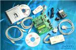


 工商网监
湘ICP备2023018690号
工商网监
湘ICP备2023018690号
