DMV1500L
®
DAMPER + MODULATION DIODE FOR VIDEO
Table 1: Main Product Characteristics
IF(AV)
DAMPER
4A
MODUL.
3A
VRRM
1500 V
600 V
trr (max)
170 ns
50 ns
VF (max)
1.5V
1.4 V
DAMPER
1
MODULATION
2
3
FEATURES AND BENEFITS
■
■
■
■
■
■
■
■
DESCRIPTION
o
r
P
e
c
u
d
3
c
u
d
Full kit in one package
High breakdown voltage capability
Very fast recovery diode
Specified turn on switching characteristics
Low static and peak forward voltage drop for
low dissipation
Insulated version:
Insulated voltage = 2000 VRMS
Capacitance = 7 pF
Planar technology allowing high quality and
best electrical characteristics
Outstanding performance of well proven DTV
as damper and new faster Turbo 2 600V
technology as modulation
(t s)
2
1
)
s
t(
TO-220FPAB
DMV1500LFD
e
t
le
o
s
b
O
-
o
r
P
2
1
3
TO-220FPAB F5 Bending
DMV1500LFD5
(optional)
High voltage semiconductor especially designed
for horizontal deflection stage in standard and high
resolution video display with E/W correction.
The insulated TO-220FPAB package includes
both the DAMPER diode and the MODULATION
diode, thanks to a dedicated design.
Assembled on automated line, it offers very low
dispersion values on insulating and thermal
performances.
t
e
l
o
s
b
O
Table 2: Order Codes
Part Number
DMV1500LFD
DMV1500LFD5
September 2004
Marking
DMV1500L
DMV1500L
REV. 1
1/9
�DMV1500L
Table 3: Absolute Maximum Ratings
Symbol
VRRM
Repetitive peak reverse voltage
IFSM
Surge non repetitive forward current
Tstg
Storage temperature range
Tj
Value
Damper
Modul.
Parameter
Unit
1500
600
V
50
35
A
tp = 10ms sinusoidal
-40 to +150
°C
150
°C
Maximum operating junction temperature
Table 4: Thermal Resistance
Symbol
Rth(j-c)
Parameter
Value
Unit
4.0
°C/W
Junction to case thermal resistance
Table 5: Static Electrical Characteristics
Value
Symbol
Parameter
Test conditions
Tj = 25°C
Typ.
IR *
Reverse leakage current
VF **
Pulse test:
Forward voltage drop
Damper
VR = 1500 V
Modul.
VR = 600 V
Damper
IF = 4 A
Modul.
IF = 3 A
* tp = 5 ms, δ < 2%
o
s
b
O
-
uc
Max.
Typ.
Max.
100
100
1000
20
d
o
r
3
50
1.7
1.1
1.5
1.8
1.1
1.4
P
e
let
1.2
)
s
t(
Tj = 125°C
Unit
µA
V
** tp = 380 µs, δ < 2%
To evaluate the maximum conduction losses of the DAMPER and MODULATION diodes use the following equations :
2
)
s
(
ct
DAMPER: P = 1.2 x IF(AV) + 0.075 x IF (RMS)
2
MODULATION: P = 1.12 x IF(AV) + 0.092 x IF (RMS)
u
d
o
Table 6: Recovery Characteristics
r
P
e
Symbol
Parameter
t
e
l
o
bs
O
2/9
trr
Reverse recovery time
Value
Test conditions
Damper
Typ.
IF = 100mA
IR =100mA
IRR = 10mA
Tj = 25°C
IF = 1A
dIF/dt = -50 A/µs
VR =30V
Tj = 25°C
Max.
850
Modul.
Typ.
Max.
110
350
Unit
ns
130
170
35
50
�DMV1500L
Table 7: Turn-On Switching Characteristics
Symbol
Parameter
Damper
tfr
Forward recovery time
Modul.
Damper
VFP
Peak forward voltage
Modul.
)
s
(
ct
450
IF = 6.5 A
dIF/dt = 50 A/µs
VFR = 3 V
Tj = 25°C
450
IF = 3 A
dIF/dt = 80 A/µs
VFR = 2 V
Tj = 100°C
240
IF = 4 A
dIF/dt = 80 A/µs
Tj = 100°C
28
IF = 6.5 A
dIF/dt = 50 A/µs
Tj = 25°C
13
IF = 3 A
dIF/dt = 80 A/µs
Tj = 100°C
r
P
e
1.6
uc
17
d
o
r
P
e
let
ns
)
s
t(
V
8
Figure 2: Average forward current versus
ambient temperature
IF(AV)(A)
7
Rth(j-a)=Rth(j-c)
6
bs
1.8
36
Unit
o
s
b
O
-
t
e
l
o
2.0
Max.
Tj = 100°C
u
d
o
PF(AV)(W)
Typ.
IF = 4 A
dIF/dt = 80 A/µs
VFR = 3 V
Figure 1: Power dissipation versus peak
forward current (triangular waveform, δ=0.45)
2.2
Value
Test conditions
DAMPER diode
5
O
1.4
4
1.2
Rth(j-a)=Rth(j-c)
1.0
3
0.8
MODULATION diode
2
0.6
T
0.4
1
0.2
IP(A)
δ=tp/T
0
0.0
0.0
0.5
1.0
1.5
2.0
2.5
3.0
3.5
4.0
4.5
5.0
5.5
6.0
0
Tamb(°C)
tp
25
50
75
100
125
150
3/9
�DMV1500L
Figure 3: Forward voltage drop versus forward
current (damper diode)
Figure 4: Forward voltage drop versus forward
current (modulation diode)
IFM(A)
IFM(A)
30
30
Tj=125°C
(maximum values)
25
Tj=125°C
(maximum values)
25
20
20
Tj=125°C
(typical values)
15
15
Tj=25°C
(maximum values)
10
Tj=125°C
(typical values)
Tj=25°C
(maximum values)
10
5
5
VFM(V)
VFM(V)
0
0
0.0
0.5
1.0
1.5
2.0
2.5
3.0
Figure 5: Relative variation of thermal
impedance junction to case versus pulse
duration
0.0
0.5
1.0
1.5
2.0
c
u
d
IM(A)
35
0.9
30
0.8
25
0.7
0.6
e
t
le
DAMPER diode
MODULATION diode
20
0.5
o
s
b
O
15
0.4
0.3
10
0.2
3.0
3.5
Figure 6: Non repetitive peak forward current
versus overload duration (damper diode)
Zth(j-c)/Rth(j-c)
1.0
2.5
o
r
P
)
s
t(
TC=25°C
TC=75°C
TC=125°C
IM
5
0.1
t
tp(s)
1.E-03
1.E-02
1.E-01
1.E+00
(s)
1.E+01
1.E+02
t
c
u
Figure 7: Non repetitive peak forward current
versus overload duration (modulation diode)
d
o
r
P
e
IM(A)
30
t
e
l
o
25
20
O
1.E-01
1.E+00
IF=IP
Tj=125°C
90% confidence
2.0
1.8
1.6
1.4
1.2
TC=75°C
1.0
0.8
IM
0.6
0.4
t
0.2
t(s)
δ=0.5
dIF/dt(A/µs)
0.0
0
4/9
1.E-02
Figure 8: Reverse recovery charges versus
dIF/dt (damper diode)
2.2
TC=125°C
1.E-03
1.E-03
Qrr(nC)
10
5
0
2.4
TC=25°C
bs
15
t(s)
δ=0.5
Single pulse
0.0
1.E-02
1.E-01
1.E+00
0.1
1.0
10.0
�DMV1500L
Figure 9: Reverse recovery charges versus
dIF /dt (modulation diode)
Figure 10: Peak reverse recovery current
versus dIF/dt (damper diode)
Qrr(nC)
IRM(A)
200
3.0
IF=IP
Tj=125°C
90% confidence
IF=IP
Tj=125°C
90% confidence
2.5
150
2.0
1.5
100
1.0
50
0.5
dIF/dt(A/µs)
dIF/dt(A/µs)
0.0
0
0.1
1.0
10.0
0.1
100.0
Figure 11: Peak reverse recovery current
versus dIF/dt (modulation diode)
1.0
10.0
IRM(A)
c
u
d
VFP(V)
6.0
50
IF=IP
Tj=125°C
90% confidence
5.0
IF=IP
Tj=125°C
90% confidence
45
40
35
4.0
e
t
le
30
3.0
25
20
2.0
)
s
t(
Figure 12: Transient peak forward voltage
versus dIF/dt (damper diode)
o
s
b
O
15
o
r
P
10
1.0
5
dIF/dt(A/µs)
dIF/dt(A/µs)
0
0.0
1
10
)
s
(
ct
100
Figure 13: Transient peak forward voltage
versus dIF/dt (modulation diode)
u
d
o
VFP(V)
11
IF=IP
Tj=125°C
90% confidence
10
8
7
5
60
80
100
120
140
Figure 14: Forward recovery time versus dIF/dt
(damper diode)
IF=IP
Tj=125°C
VFR=3V
90% confidence
650
600
550
500
s
b
O
6
40
700
t
e
l
o
9
20
tfr(ns)
r
P
e
12
0
1000
450
400
4
350
3
300
2
1
250
dIF/dt(A/µs)
0
dIF/dt(A/µs)
200
0
20
40
60
80
100
120
140
160
180
200
0
20
40
60
80
100
120
140
5/9
�DMV1500L
Figure 15: Forward recovery time versus dIF/dt
(modulation diode)
Figure 16: Relative variation of dynamic
parameters versus junction temperature
IRM, VFP, QRR [Tj]/ IRM, VFP, QRR [Tj=125°C]
tfr(ns)
1.2
200
IF=IP
Tj=125°C
VFR=2V
90% confidence
175
1.0
150
0.8
125
VFP
0.6
100
IRM
75
0.4
QRR
50
0.2
25
Tj(°C)
dIF/dt(A/µs)
0
0.0
0
20
40
60
80
100
120
140
160
180
200
25
50
75
100
Figure 17: Junction capacitance versus
reverse voltage applied (typical values)
c
u
d
C(pF)
100
F=1MHz
VOSC=30mVRMS
Tj=25°C
MODULATION diode
10
e
t
le
DAMPER diode
VR(V)
1
1
10
)
s
(
ct
100
u
d
o
r
P
e
t
e
l
o
s
b
O
6/9
o
s
b
O
-
1000
o
r
P
125
)
s
t(
�DMV1500L
Figure 18: TO-220FPAB Package Mechanical Data
REF.
A
B
D
E
F
F1
F2
G
G1
H
L2
L3
L4
L6
L7
Dia.
DIMENSIONS
Millimeters
Inches
Min.
Max.
Min.
Max.
4.4
4.9
0.173
0.192
2.5
2.9
0.098
0.114
2.45
2.75
0.096
0.108
0.4
0.7
0.016
0.027
0.6
1
0.024
0.039
1.15
1.7
0.045
0.067
1.15
1.7
0.045
0.067
4.95
5.2
0.195
0.205
2.4
2.7
0.094
0.106
10
10.7
0.393
0.421
16 Typ.
0.630 Typ.
28.6
30.6
1.126
1.205
9.8
10.7
0.385
0.421
15.8
16.4
0.622
0.646
9
9.9
0.354
0.390
2.9
3.5
0.114
0.138
c
u
d
e
t
le
)
s
(
ct
)
s
t(
o
r
P
o
s
b
O
-
u
d
o
r
P
e
t
e
l
o
s
b
O
7/9
�DMV1500L
Figure 19: TO-220FPAB F5 Bending (option) Package Mechanical Data
REF.
A
B
D
E
F
F1
F2
G
G1
H
L2
L3
L4
L6
L7
M1
R
Dia.
Table 8: Ordering Information
Part Number
Marking
DMV1500LFD
DMV1500LFD5
DMV1500L
DMV1500L
r
P
e
Date
07-Sep-2004
t
e
l
o
s
b
O
8/9
e
t
le
Weight
Base qty
TO-220FPAB
TO-220FPAB F5
2.4 g
2.4 g
50
45
Description of Changes
First issue
)
s
t(
o
r
P
Package
)
s
(
ct
Revision
1
c
u
d
o
s
b
O
-
u
d
o
Table 9: Revision History
DIMENSIONS
Millimeters
Inches
Min.
Max.
Min.
Max.
4.4
4.9
0.173
0.192
2.5
2.9
0.098
0.114
2.45
2.75
0.096
0.108
0.4
0.7
0.016
0.027
0.6
1
0.024
0.039
1.15
1.7
0.045
0.067
1.15
1.7
0.045
0.067
4.95
5.2
0.195
0.205
2.4
2.7
0.094
0.106
10
10.7
0.393
0.421
16 Typ.
0.630 Typ.
24.16
26.9
0.951
1.059
1.65
2.41
0.065
0.095
15.8
16.4
0.622
0.646
9
9.9
0.354
0.390
2.92
3.3
0.115
0.130
1.4 Typ.
0.055 Typ.
2.9
3.5
0.114
0.138
Delivery
mode
Tube
Tube
�DMV1500L
c
u
d
e
t
le
)
s
(
ct
)
s
t(
o
r
P
o
s
b
O
-
u
d
o
r
P
e
t
e
l
o
s
b
O
Information furnished is believed to be accurate and reliable. However, STMicroelectronics assumes no responsibility for the consequences
of use of such information nor for any infringement of patents or other rights of third parties which may result from its use. No license is granted
by implication or otherwise under any patent or patent rights of STMicroelectronics. Specifications mentioned in this publication are subject
to change without notice. This publication supersedes and replaces all information previously supplied. STMicroelectronics products are not
authorized for use as critical components in life support devices or systems without express written approval of STMicroelectronics.
The ST logo is a registered trademark of STMicroelectronics.
All other names are the property of their respective owners
© 2004 STMicroelectronics - All rights reserved
STMicroelectronics group of companies
Australia - Belgium - Brazil - Canada - China - Czech Republic - Finland - France - Germany - Hong Kong - India - Israel - Italy - Japan Malaysia - Malta - Morocco - Singapore - Spain - Sweden - Switzerland - United Kingdom - United States of America
www.st.com
9/9
�
很抱歉,暂时无法提供与“DMV1500LF5”相匹配的价格&库存,您可以联系我们找货
免费人工找货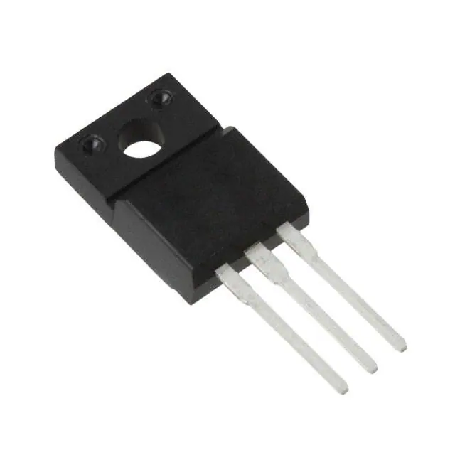


 工商网监
湘ICP备2023018690号
工商网监
湘ICP备2023018690号
