ECMF4-2450A17M10
Common mode filter with ESD protection for high speed serial interface
Datasheet - production data
Description
The ECMF4-2450A17M10 is a highly integrated
common mode filter and low pass filter designed
to suppress WiFi differential and common mode
noise on high speed differential serial buses like
HDMI. The device can protect and filter 2
differential lanes.
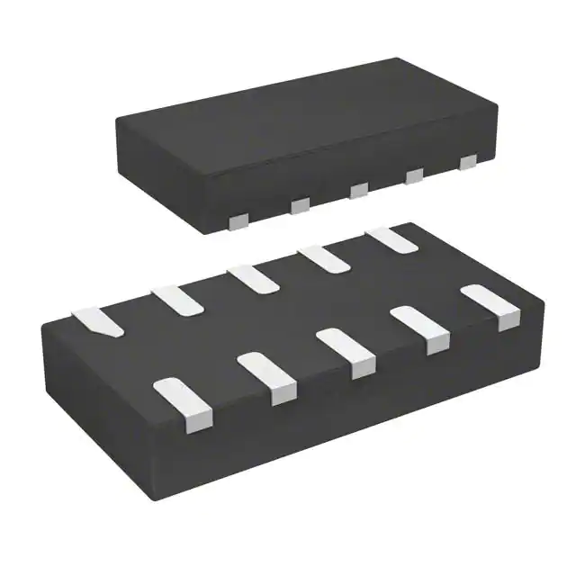
Figure 1: Pin configuration
µQFN-10L 2.60 x 1.35 mm
Features
High differential mode attenuation on WLAN
frequencies :
-23 dB at 2.4 GHz and -32 dB at
5.0 GHz
Large bandwidth: 1.7 GHz
Very low PCB space consumption.
Thin package: 0.55 mm max.
Lead-free package.
High reduction of parasitic elements through
integration.
D1+
1
10
D1+
D1-
2
9
D1-
GND
3
8
GND
D2+
4
7
D2+
D2-
5
6
D2-
Applications
Set top box
Streaming box
HDMI stick
Game console
Notebook, laptop
Portable devices
November 2016
DocID030008 Rev 1
This is information on a product in full production.
1/13
www.st.com
�Characteristics
1
ECMF4-2450A17M10
Characteristics
Table 1: Absolute maximum ratings (Tamb = 25 °C)
Symbol
Parameter
Value
Unit
8
15
kV
mA
IEC 61000-4-2:
Contact discharge (connector side)
Air discharge (connector side)
VPP
Peak pulse voltage
IRMS
Maximum RMS current
100
Top
Operating temperature
-40 to +85
Tj
Maximum junction temperature
Tstg
125
Storage temperature range
°C
-55 to +150
Figure 2: Electrical characteristics (definitions)
Table 2: Electrical characteristics (Tamb = 25 °C)
Symbol
Test condition
Min.
Typ.
4.5
5.5
Unit
VBR
IR = 1 mA
IRM
VRM = 3 V per line
RDC
DC serial resistance
5.5
Ω
-3 dB differential mode cut-off frequency
1.7
GHz
Fc
Cdiode
[D+ or D-]/ GND
Rd
nA
10
IEC 61000 4-2, +8 kV contact (IPP = 16 A),
measured at 30 ns
12.9
VD+/D- = 0 V, F = 2.5 GHz to 6 GHz
0.35
Dynamic resistance,
tP = 100 ns
V
100
IPP = 1 A, 8/20 µs
VCL
2/13
Max.
D+ or D- to GND
0.48
GND to D+ or D-
0.96
DocID030008 Rev 1
V
0.45
pF
Ω
�ECMF4-2450A17M10
Characteristics
Table 3: Pin description
Pin number
Description
Pin number
Description
1
D1+ (to connector)
6
D2- (to IC)
2
D1- (to connector)
7
D2+ (to IC)
3
GND
8
GND
4
D2+(to connector)
9
D1- (to IC)
5
D2- (to connector)
10
D1+ (to IC)
DocID030008 Rev 1
3/13
�Characteristics
1.1
ECMF4-2450A17M10
Characteristics (curves)
Figure 3: Differential attenuation versus frequency (Z0 diff = 100 Ω) – evaluation board with SMA connector
Figure 4: Common mode attenuation versus frequency (Z0 com = 50 Ω)
Figure 5: ESD response to IEC61000-4-2 (+8 kV contact discharge)
4/13
DocID030008 Rev 1
�ECMF4-2450A17M10
Characteristics
Figure 6: ESD response to IEC61000-4-2 (-8 kV contact discharge)
Figure 7: HDMI1.4 2.228 Gbps source eye diagram
(without ECMF4-2450A17M10)
Figure 8: HDMI1.4 2.228 Gbps source eye diagram
(with ECMF4-2450A17M10)
Figure 9: HDMI1.4 1.485 Gbps source eye diagram
(without ECMF4-2450A17M10)
Figure 10: HDMI1.4 1.485 Gbps source eye diagram
(with ECMF4-2450A17M10)
DocID030008 Rev 1
5/13
�Application information
2
ECMF4-2450A17M10
Application information
Figure 11: HDMI schematic
ECMF4-2450A17M10
D0
ECMF4-2450A17M10
HDMI ASIC
HDMI connector
D1
D2
CLK
HDMI2C1-6C1
6/13
DocID030008 Rev 1
�Package information
ECMF4-2450A17M10
3
Package information
In order to meet environmental requirements, ST offers these devices in different grades of
ECOPACK® packages, depending on their level of environmental compliance. ECOPACK®
specifications, grade definitions and product status are available at: www.st.com.
ECOPACK® is an ST trademark.
3.1
µQFN10L package information
Figure 12: µQFN10L package outline
Table 4: µQFN10L package mechanical data
Dimensions
Ref.
Millimeters
Inches
Min.
Typ.
Max.
Min.
Typ.
Max.
A
0.45
0.50
0.55
0.018
0.020
0.022
A1
0.00
0.02
0.05
0.00
0.0008
0.002
b
0.15
0.20
0.25
0.006
0.008
0.010
D
2.55
2.60
2.65
0.1
0.102
0.104
E
1.30
1.35
1.40
0.051
0.053
0.055
e
L
0.50
0.40
0.50
0.020
0.60
DocID030008 Rev 1
0.016
0.020
0.024
7/13
�Package information
ECMF4-2450A17M10
Figure 14: Marking layout
Figure 13: Footprint recommendations,
dimensions in mm (inches)
0.20
0.70
ME
1.75
0.50
Product marking may be rotated by 90° for assembly plant differentiation. In no
case should this product marking be used to orient the component for its
placement on a PCB. Only pin 1 mark is to be used for this purpose.
Figure 16: Tape and reel orientation
Figure 15: Package orientation in reel
Figure 17: Reel dimensions in mm
8/13
Figure 18: Inner box dimension definition in mm
DocID030008 Rev 1
�Package information
ECMF4-2450A17M10
Figure 19: Tape dimension definitions
Table 5: Tape and reel mechanical data
Dimensions
Ref.
P1
Millimeters
Min.
Typ.
Max.
3.9
4.0
4.1
P0
4.0
Ø D0
1.4
1.5
1.6
Ø D1
1
F
3.45
3.5
3.55
K0
0.6
0.7
0.8
P2
1.95
2
2.05
W
7.9
8
8.3
DocID030008 Rev 1
9/13
�Recommendation on PCB assembly
ECMF4-2450A17M10
4
Recommendation on PCB assembly
4.1
Solder paste
1.
2.
3.
4.
4.2
Placement
1.
2.
3.
4.
5.
6.
4.3
Manual positioning is not recommended.
It is recommended to use the lead recognition capabilities of the placement system,
not the outline centering
Standard tolerance of ±0.05 mm is recommended.
3.5 N placement force is recommended. Too much placement force can lead to
squeezed out solder paste and cause solder joints to short. Too low placement force
can lead to insufficient contact between package and solder paste that could cause
open solder joints or badly centered packages.
To improve the package placement accuracy, a bottom side optical control should be
performed with a high resolution tool.
For assembly, a perfect supporting of the PCB (all the more on flexible PCB) is
recommended during solder paste printing, pick and place and reflow soldering by
using optimized tools.
PCB design preference
1.
2.
10/13
Halide-free flux qualification ROL0 according to ANSI/J-STD-004.
“No clean” solder paste is recommended.
Offers a high tack force to resist component movement during high speed.
Solder paste with fine particles: powder particle size is 20-45 μm.
To control the solder paste amount, the closed via is recommended instead of open
vias.
The position of tracks and open vias in the solder area should be well balanced. The
symmetrical layout is recommended, in case any tilt phenomena caused by
asymmetrical solder paste amount due to the solder flow away.
DocID030008 Rev 1
�Recommendation on PCB assembly
ECMF4-2450A17M10
4.4
Reflow profile
Figure 20: ST ECOPACK® recommended soldering reflow profile for PCB mounting
Minimize air convection currents in the reflow oven to avoid component
movement.
Maximum soldering profile corresponds to the latest IPC/JEDEC J-STD-020.
DocID030008 Rev 1
11/13
�Ordering information
5
ECMF4-2450A17M10
Ordering information
Figure 21: Ordering information scheme
ECMF 4 – 24 50 A 17 M10
Function
Common mode filter with ESD protection
Number of lines
4 = 4 filtered lines with ESD protection
1st common mode rejection
24 = 2.4 GHz
2nd common mode rejection
50 = 5.0 GHz
Version
A = 1st version
Differential bandwidth
17 = 1.7 GHz
Package
M10: µQFN-10L
Table 6: Ordering information
6
Order code
Marking
Package
Weight
Base qty.
Delivery mode
ECMF4-2450A17M10
ME
µQFN-10L
5 mg
3000
Tape and reel
Revision history
Table 7: Document revision history
12/13
Date
Revision
08-Nov-2016
1
Changes
Initial release.
DocID030008 Rev 1
�ECMF4-2450A17M10
IMPORTANT NOTICE – PLEASE READ CAREFULLY
STMicroelectronics NV and its subsidiaries (“ST”) reserve the right to make changes, corrections, enhancements, modifications, and
improvements to ST products and/or to this document at any time without notice. Purchasers should obtain the latest relevant information on ST
products before placing orders. ST products are sold pursuant to ST’s terms and conditions of sale in place at the time of order
acknowledgement.
Purchasers are solely responsible for the choice, selection, and use of ST products and ST assumes no liability for application assistance or the
design of Purchasers’ products.
No license, express or implied, to any intellectual property right is granted by ST herein.
Resale of ST products with provisions different from the information set forth herein shall void any warranty granted by ST for such product.
ST and the ST logo are trademarks of ST. All other product or service names are the property of their respective owners.
Information in this document supersedes and replaces information previously supplied in any prior versions of this document.
© 2016 STMicroelectronics – All rights reserved
DocID030008 Rev 1
13/13
�
很抱歉,暂时无法提供与“ECMF4-2450A17M10”相匹配的价格&库存,您可以联系我们找货
免费人工找货- 国内价格
- 1+2.26760
- 200+1.88960
- 500+1.51170
- 1000+1.25980