EMIF02-USB03F2
2-line IPAD™, EMI filter including ESD protection
Datasheet - production data
Description
The EMIF02-USB03F2 is a highly integrated
array designed to suppress EMI / RFI noise for
USB OTG (on-the-go) ports.
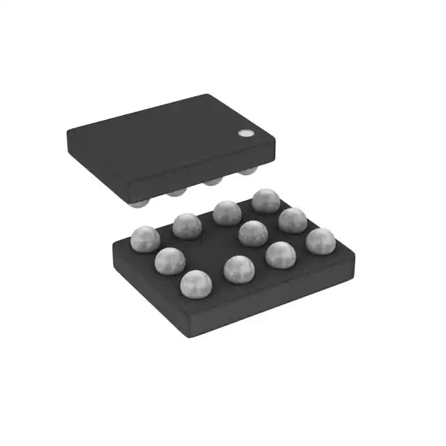
The EMIF02-USB03F2 Flip-Chip packaging
means the package size is equal to the die size.
Additionally, this filter includes ESD protection
circuitry which prevents damage to the protected
device when subjected to ESD surges up to 15 kV
on external contacts.
)OLS�&KLS�SDFNDJH
����EXPSV�
Figure 1.
Pin layout (bump side)
Features
3
2
• 2-line, low-pass filter + 2-line ESD protection
ID
Dz
Vbus
Pup
Pd1
B
D+
out
Pd2
D+
in
C
Dout
GND
Din
D
1
A
• High efficiency in EMI filtering
• Lead-free package
• Very low PCB space occupation: < 2.80 mm2
• Very thin package: 0.65 mm
• High efficiency in ESD suppression
(IEC 61000-4-2 level 4)
• High reliability offered by monolithic integration
Figure 2. Schematic
• High reduction of parasitic elements through
integration and wafer level packaging
Pup
Dz
ID
Vbus
EMIF02-USB03F2
R3=1.3kΩ
Complies with the following standards
• IEC 61000-4-2 level 4 on external pins:
– 15 kV (air discharge)
– 8 kV (contact discharge)
• IEC 61000-4-2 level 1 on internal pins:
– 2 kV (air discharge)
– 2 kV (contact discharge)
D+OUT
R2=33Ω
D+IN
D-OUT
R1=33Ω
D-IN
R5=15kΩ
R4=17kΩ
Pd2
Pd1
CLINE = 20 pF max.
Application
ESD protection and EMI filtering for:
• USB OTG port
September 2015
This is information on a product in full production.
TM: IPAD is a trademark of STMicroelectronics.
DocID10740 Rev 6
1/8
www.st.com
�Characteristics
1
EMIF02-USB03F2
Characteristics
Table 1.
Absolute ratings (Tamb = 25 °C)
Symbol
Parameter and test conditions
Value
Unit
Internal pins (D3, C3, C2, B2, B1):
ESD discharge IEC61000-4-2, air discharge
ESD discharge IEC61000-4-2, contact discharge
External pins (D1, C1, A2, A3, B3):
ESD discharge IEC61000-4-2, air discharge
ESD discharge IEC61000-4-2, contact discharge
15
8
Tj
Maximum junction temperature
125
°C
Top
Operating temperature range
-40 to +85
°C
Tstg
Storage temperature range
-55 to 150
°C
VPP
2
2
kV
Figure 3. Electrical characteristics (definitions)
3DUDPHWHU
6\PERO 3DUDPHWHUV
9%5��� ��%UHDNGRZQ�YROWDJH
,50���� ��/HDNDJH�FXUUHQW�DW�950
950��� �6WDQG�RII�YROWDJH
9&/���� �&ODPSLQJ�YROWDJH
5G������� �'\QDPLF�LPSHGHQFH
,33������ �3HDN�SXOVH�FXUUHQW
&/,1(� �,QSXW�FDSDFLWDQFH�SHU�OLQH
Table 2. Electrical characteristics (Tamb = 25 °C)
Symbol
2/8
Conditions
Min.
Typ.
Max.
Unit
VBR
IR = 1 mA
IRM
VRM = 3 V
0.2
µA
CLINE
VLINE = 0 V, VOSC = 30 mV, F = 1 MHz,
measured in zero light condition
20
pF
R1, R2
Tolerance ± 5%
33
Ω
R3
Tolerance ± 5%
1.30
kΩ
R4
Tolerance ± 5%
17
kΩ
R5
Tolerance ± 5%
15
kΩ
14
DocID10740 Rev 6
V
�EMIF02-USB03F2
Characteristics
Figure 4. Filtering measurement
0
Figure 5. Analog crosstalk measurement
0 dB
-10
-20
-30
-40
-50
-60
-70
-80
-90
-100
-110
-120
-130
dB
-10
-20
-30
F (Hz)
-40
100k
1M
D+In D+Out
10M
100M
D-In D-Out
1G
F (Hz)
100k
1M
D-In D+Out
Figure 6. ESD response to IEC 61000-4-2
(+15 kV air discharge)
on one input VIN and on one output VOUT
10M
100M
DZ ID
1G
Figure 7. ESD response to IEC 61000-4-2
(-15 kV air discharge)
on one input VIN and on one output VOUT
10.0 V / Div.
20.0 V / Div.
VCL = 74 V
IN
IN
VCL = -47 V
100 ns / Div.
100 ns / Div.
10.0 V / Div.
10.0 V / Div.
VCL = 27 V
OUT
OUT
VCL = -23 V
100 ns / Div.
100 ns / Div.
Figure 8. Junction capacitance versus reverse voltage applied (typical values)
C(pF)
20
18
16
14
12
10
8
6
4
2
VLINE (V)
0
0
1
2
3
4
5
6
7
DocID10740 Rev 6
8
9
10
11
12
3/8
8
�Application information
2
EMIF02-USB03F2
Application information
Figure 9. Application schematic
Vbus
Vbus
ID
ID
USB OTG Xceiver
Pup
Dz
ID
Vbus
EMIF02-USB03F2
R3=1.3kΩ
D+
D+OUT
R2=33Ω
D+IN
D-OUT
R1=33Ω
D-IN
D+
D-
R5=15kΩ
D-
R4=17kΩ
GND
USB OTG connector
3.3V
GND
Pd2
Pd1
R1 = R2 = 33 Ω
Cline = 20 pF max.
Figure 10. Aplac model
C1
C3
Ls
Rs
Lbump Rbump
Rbump Lbump
Rs
Ls
Port2
Port1
50
50
A3
A2
B3
B2
B1
D2
C2
MODEL = D02_usb03_gnd
MODEL = D02_usb03
bulk
bulk
bulk
bulk
bulk
bulk
bulk
B2 B1
R_17k
R_1k3
C3
C2
R_33R
C1
D2
R_15k
D3
R_33R
Lbump
D1
Rbump
MODEL = D02_usb03
MODEL = D02_usb03
Cgnd
Lgnd
bulk
Cbump Rsubump
A2
B1
bulk
C1
bulk
D3
bulk
Cbump Rsubump
bulk
D1
Cbump Rsubump
B3
bulk
Cbump Rsubump
Cbump Rsubump
C3
bulk
Cbump Rsubump
Cbump Rsubump
C2
Rgnd
Cbump Rsubump
bulk
Cbump Rsubump
B2
bulk
bulk
bulk
bulk
Cbump Rsubump
bulk
A3
bulk
Figure 11. Aplac parameters
Ls 950pH
Rs 150m
R_33R 33
R_1k3 1.3k
R_15k 15k
R_17k 17k
Cz_usb03 11pF
Rs_usb03 1
Cz_usb03_gnd 220pF
4/8
DocID10740 Rev 6
Rs_usb03_gnd 0.9
Lgnd 50pH
Rgnd 100m
Cgnd 0.15pF
Lbump 50pH
Rbump 20m
Cbump 2.4pF
Rsubump 100m
�EMIF02-USB03F2
3
Package information
Package information
In order to meet environmental requirements, ST offers these devices in different grades of
ECOPACK® packages, depending on their level of environmental compliance. ECOPACK®
specifications, grade definitions and product status are available at: www.st.com.
ECOPACK® is an ST trademark.
Flip-Chip package information
Figure 12. Flip-Chip package outline
315 µm ± 50
650 µm ± 65
1.94 mm ± 30 µm
500 µm
500 µm
220 µm
1.44 mm ± 30 µm
DocID10740 Rev 6
220 µm
3.1
5/8
8
�Package information
3.2
EMIF02-USB03F2
Packing information
Figure 13. Flip-Chip tape and reel outline
Dot identifying Pin A1 location
3.5 ± 0.1
xxz
yww
ST E
1.58
xxz
yww
Note:
ST E
xxz
yww
ST E
8 ± 0.3
2.04
0.73 ± 0.05
All dimensions in mm
1.75 ± 0.1
Ø 1.5 ± 0.1
4 ± 0.1
4 ± 0.1
User direction of unreeling
More information is available in the application notes:
AN1235:”Flip Chip: Package description and recommendations for use”
AN1751: “EMI filters: Recommendations and measurements”
Figure 14. Footprint
&RSSHU�SDG��'LDPHWHU�
����P�UHFRPPHQGHG�����P�PD[�
Figure 15. Marking
Dot, ST logo
ECOPACK status
xx = marking
z = manufacturing location
yww = datecode
(y = year
ww = week)
x x z
y ww
6ROGHU�VWHQFLO�RSHQLQJ�������P�UHFRPPHQGHG
6ROGHU�PDVN�RSHQLQJ�UHFRPPHQGDWLRQ�
����P�PLQ�IRU�����P�FRSSHU�SDV�GLDPHWHU��
6/8
DocID10740 Rev 6
�EMIF02-USB03F2
4
Ordering information
Ordering information
Figure 16. Ordering information scheme
EMIF
yy
-
xxx zz
Fx
EMI Filter
Number of lines
Information
x = resistance value (ohm)
z = capacitance value / 10 (pF)
or
3 letters = application
2 digits = version
Package
F = Flip Chip
x = 2: lead-free, pitch = 500 µm, bump = 315 µm
Table 3. Ordering information
5
Order code
Marking
Package
Weight
Base qty
Delivery mode
EMIF02-USB03F2
FU
Flip Chip
4 mg
5000
Tape and reel 7”
Revision history
Table 4. Document revision history
Date
Revision
Changes
14-Oct-2004
1
Initial release.
25-Oct-2004
2
Figure 12: Flip Chip marking dimensions updated.
27-Oct-2004
3
Minor layout update. No content change.
28-Apr-2008
4
Updated ECOPACK statement. Updated Figure 12, Figure 13,
Figure 14, Figure 15 and Figure 16 Reformatted to current standards.
08-Feb-2010
5
Updated the maximum value of IRM in Table 2. Updated Figure 12 and
Figure 13 for die dimension reductions.
15-Sep-2015
6
Updated Figure 14 and reformatted to current standards.
DocID10740 Rev 6
7/8
8
�EMIF02-USB03F2
IMPORTANT NOTICE – PLEASE READ CAREFULLY
STMicroelectronics NV and its subsidiaries (“ST”) reserve the right to make changes, corrections, enhancements, modifications, and
improvements to ST products and/or to this document at any time without notice. Purchasers should obtain the latest relevant information on
ST products before placing orders. ST products are sold pursuant to ST’s terms and conditions of sale in place at the time of order
acknowledgement.
Purchasers are solely responsible for the choice, selection, and use of ST products and ST assumes no liability for application assistance or
the design of Purchasers’ products.
No license, express or implied, to any intellectual property right is granted by ST herein.
Resale of ST products with provisions different from the information set forth herein shall void any warranty granted by ST for such product.
ST and the ST logo are trademarks of ST. All other product or service names are the property of their respective owners.
Information in this document supersedes and replaces information previously supplied in any prior versions of this document.
© 2015 STMicroelectronics – All rights reserved
8/8
DocID10740 Rev 6
�
很抱歉,暂时无法提供与“EMIF02-USB03F2”相匹配的价格&库存,您可以联系我们找货
免费人工找货