1. 物料型号:
- ESDA6V1P6
- ESDA6V1-5P6
- ESDA14V2BP6
2. 器件简介:
- ESDAxxxP6系列是单片数组,用于保护多达5条线路免受ESD瞬态影响。这些器件非常适合需要降低线路电容和节省板空间的情况。
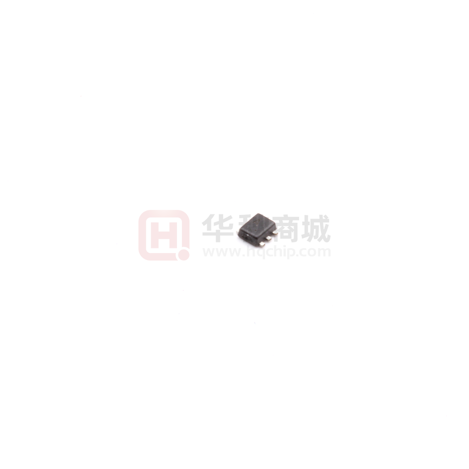
3. 引脚分配:
- SOT-666IP(内部焊盘):ESDA6V1P6、ESDA6V1-5P6
- SOT-666:ESDA14V2BP6
4. 参数特性:
- 击穿电压:ESDA6V1P6/ESDA6V1-5P6为6.1V最小,ESDA14V2BP6为14.2V最小。
- 低漏电流:ESDA6V1P6/ESDA6V1-5P6小于500nA,ESDA14V2BP6小于1mA。
- 非常小的PCB面积:小于2.6mm²。
5. 功能详解:
- 这些器件特别适用于需要对称信号保护的场合,如计算机、打印机、通信系统和手机、视频设备等。
- 提供单向和双向的Transil(ESDA14V2BP6)功能。
6. 应用信息:
- 适用于需要瞬态过电压保护的ESD敏感设备,如计算机、打印机、通信系统和手机、视频设备等。
7. 封装信息:
- 提供了SOT-666IP和SOT-666两种封装类型。