ESDA25P35-1U1M
High power transient voltage suppressor
Datasheet - production data
Description
The ESDA25P35-1U1M is an unidirectional
single line TVS diode designed to protect the
power line against EOS and ESD transients.
n1
Pi
The device is ideal for applications where high
power TVS and board space saving are required.
n2
Pi
Figure 1: Pin configuration
Low clamping voltage
Typical peak pulse power: 1400 W (8/20 µs)
Stand-off voltage 22 V
Unidirectional diode
Low leakage current: 0.2 µA at 25 °C
Complies with IEC 61000-4-2 level 4
±30 kV (air discharge)
±30 kV (contact discharge)
Pin2
Features
Pin1
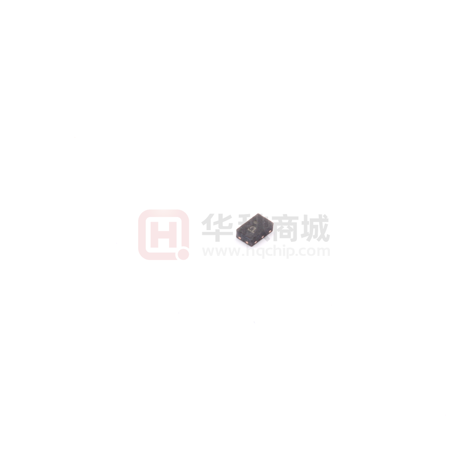
1610 package
Applications
Where transient overvoltage protection in ESD
sensitive equipment is required, such as:
Smartphones, mobile phones, tablets,
portable multimedia
USB VBUS protection
Power supply protection
Battery protection
July 2017
DocID029556 Rev 2
This is information on a product in full production.
1/9
www.st.com
�Characteristics
1
ESDA25P35-1U1M
Characteristics
Table 1: Absolute maximum ratings (Tamb = 25 °C)
Symbol
Parameter
Value
Unit
VPP
Peak pulse voltage
IEC 61000-4-2:
Contact discharge
Air discharge
>30
>30
kV
PPP
Peak pulse power
8/20μs
1400
W
IPP
Peak pulse current
8/20μs
35
A
Tstg
Storage junction temperature range
-55 to +150
Maximum operating junction temperature
-55 to +150
Tj
°C
Figure 2: Electrical characteristics (definitions)
Table 2: Electrical characteristics (Tamb = 25 °C)
Symbol
VBR
Test condition
IR = 1 mA
Min.
Typ.
Max.
23.3
24.6
25.8
VRM
VRM = 22 V
Rd
8/20 µs
VF
2/9
V
22
IRM
VCL
Unit
200
Ω
0.45
IPP = 35 A; 8/20 µs
39
41
IPP = 10 A; 8/20 µs
29
31
IF = 10 mA
0.75
DocID029556 Rev 2
nA
V
V
�ESDA25P35-1U1M
1.1
Characteristics
Characteristics (curves)
Figure 3: Peak power dissipation versus initial
temperature (typical value)
1500
Figure 4: Peak pulse power versus exponential
pulse duration (Tj initial = 25°C) (typical value)
PPP (W)
PPP (W)
Tj initial = 25 °C
typical value
8/20µs
typical value
1000
1250
1000
100
750
Tj(°C)
500
25
50
75
100
125
150
10
175
Figure 5: Clamping voltage versus peak pulse
current (max. value)
100.00
100
1000
Figure 6: Leakage current versus junction
temperature (typical value)
IR(nA)
IPP (A)
35
8/20 µs
T j initial = 25 °C
tp(µs)
10
VR = VRM = 22 V
reverse
typical value
30
25
10.00
20
15
1.00
10
5
0.10
20.00
VCL(V)
25.00
30.00
35.00
40.00
45.00
Tj(°C)
0
25
Figure 7: ESD response to IEC 61000-4-2
(+8kV contact discharge)
50
75
100
125
150
Figure 8: ESD response to IEC 61000-4-2
(-8kV contact discharge)
5 V/div
10 V/div
20 ns/div
20 ns/div
ESD level
V pp
V CL @ 30ns
V CL @ 60ns
V CL @ 100ns
ESD level
V pp
V CL @ 30ns
V CL @ 60ns
V CL @ 100ns
+8kV
45V
26V
27V
27V
-8kV
-16.2V
-1.8V
-1.2V
-0.8V
DocID029556 Rev 2
3/9
�Package information
2
ESDA25P35-1U1M
Package information
In order to meet environmental requirements, ST offers these devices in different grades of
ECOPACK® packages, depending on their level of environmental compliance. ECOPACK®
specifications, grade definitions and product status are available at: www.st.com.
ECOPACK® is an ST trademark.
2.1
QFN 1610 package information
Figure 9: QFN 1610 package outline
E
D
A
Top view
A1
Side view
b
e
L
Bottom view
Table 3: QFN 1610 package mechanical data
Dimensions
Ref.
A
Millimeters
Min.
Typ.
Max.
Min.
Typ.
Max.
0.51
0.55
0.60
0.0201
0.0217
0.0236
0.02
0.05
0.0008
0.0020
0.80
0.85
0.0315
0.0335
A1
b
0.75
0.0295
D
1.60
0.0630
E
1.00
0.0394
e
1.05
0.0413
L
4/9
Inches
0.30
0.35
0.40
DocID029556 Rev 2
0.011
0.013
0.015
�Package information
ESDA25P35-1U1M
Figure 10: Footprint recommendations
Figure 11: Alternative footprint dimensions
Figure 12: Marking
P
Pin2
Pin1
Product marking may be rotated by multiples of 90° for assembly plant
differentiation. In no case should this product marking be used to orient the
component for its placement on a PCB. Only pin 1 mark is to be used for this
purpose.
Figure 13: Tape and reel specification
2.0 ±0.05
Ø 1.50 +0.10
4.0 ±0.10
1.75 ±0.10
Bar indicates Pin1
1.14 ±0.03
0.67 ±0.05
P
P
P
P
P
P
P
3.50 ±0.05
1.75 ±0.03
8.0 ±0.10
0.20 ±0.02
2.0 ±0.10
All dimensions are typical values in mm
User direction of unreeling
DocID029556 Rev 2
5/9
�Recommendation on PCB assembly
ESDA25P35-1U1M
3
Recommendation on PCB assembly
3.1
Stencil opening design
1.
2.
General recommendation on stencil opening design
a. Stencil opening dimensions: L (Length), W (Width), T (Thickness).
General design rule
a. Stencil thickness (T) = 75 ~ 125 μm
𝑊
b. Aspect ratio = ≥ 1.5
𝑇
c.
3.
Aspect area =
𝐿×𝑊
2𝑇(𝐿+𝑊)
≥ 0.66
Reference design
a. Stencil opening thickness: 100 μm
b. Stencil opening for leads: Opening to footprint ratio is 90%.
Figure 14: Stencil opening dimensions
Figure 15: Recommended stencil window position
3.2
Solder paste
1.
2.
3.
4.
6/9
Figure 16: Alternative stencil window position
Halide-free flux qualification ROL0 according to ANSI/J-STD-004.
“No clean” solder paste is recommended.
Offers a high tack force to resist component movement during high speed.
Solder paste with fine particles: powder particle size is 20-38 μm.
DocID029556 Rev 2
�Recommendation on PCB assembly
ESDA25P35-1U1M
3.3
Placement
1.
2.
3.
4.
5.
6.
3.4
PCB design preference
1.
2.
3.5
Manual positioning is not recommended.
It is recommended to use the lead recognition capabilities of the placement system,
not the outline centering
Standard tolerance of ±0.05 mm is recommended.
3.5 N placement force is recommended. Too much placement force can lead to
squeezed out solder paste and cause solder joints to short. Too low placement force
can lead to insufficient contact between package and solder paste that could cause
open solder joints or badly centered packages.
To improve the package placement accuracy, a bottom side optical control should be
performed with a high resolution tool.
For assembly, a perfect supporting of the PCB (all the more on flexible PCB) is
recommended during solder paste printing, pick and place and reflow soldering by
using optimized tools.
To control the solder paste amount, the closed via is recommended instead of open
vias.
The position of tracks and open vias in the solder area should be well balanced. A
symmetrical layout is recommended, to avoid any tilt phenomena caused by
asymmetrical solder paste due to solder flow away.
Reflow profile
Figure 17: ST ECOPACK® recommended soldering reflow profile for PCB mounting
Minimize air convection currents in the reflow oven to avoid component
movement.
Maximum soldering profile corresponds to the latest IPC/JEDEC J-STD-020.
DocID029556 Rev 2
7/9
�Ordering information
4
ESDA25P35-1U1M
Ordering information
Figure 18: Ordering information scheme
ESDA
25 P35 - 1U1 M
ESD Array
Breakdown voltage
25 = 25 V typ.
IPP 8/20 µs
P35 = 35 A
Direction
1U1 = Unidirectional
Package
M = QFN
Table 4: Ordering information
Order code
Marking(1)
Package
Weight
Base qty.
Delivery mode
ESDA25P35-1U1M
P
QFN 1610
2.4 mg
8000
Tape and reel
Notes:
(1)The
5
marking can be rotated by multiples of 90° to differentiate assembly location
Revision history
Table 5: Document revision history
8/9
Date
Revision
Changes
28-Jul-2016
1
Initial release.
19-Jul-2017
2
Updated Table 3: "QFN 1610 package mechanical data"
DocID029556 Rev 2
�ESDA25P35-1U1M
IMPORTANT NOTICE – PLEASE READ CAREFULLY
STMicroelectronics NV and its subsidiaries (“ST”) reserve the right to make changes, corrections, enhancements, modifications, and
improvements to ST products and/or to this document at any time without notice. Purchasers should obtain the latest relevant information on ST
products before placing orders. ST products are sold pursuant to ST’s terms and conditions of sale in place at the time of order
acknowledgement.
Purchasers are solely responsible for the choice, selection, and use of ST products and ST assumes no liability for application assistance or the
design of Purchasers’ products.
No license, express or implied, to any intellectual property right is granted by ST herein.
Resale of ST products with provisions different from the information set forth herein shall void any warranty granted by ST for such product.
ST and the ST logo are trademarks of ST. All other product or service names are the property of their respective owners.
Information in this document supersedes and replaces information previously supplied in any prior versions of this document.
© 2017 STMicroelectronics – All rights reserved
DocID029556 Rev 2
9/9
�
很抱歉,暂时无法提供与“ESDA25P35-1U1M”相匹配的价格&库存,您可以联系我们找货
免费人工找货- 国内价格 香港价格
- 8000+0.699388000+0.08676
- 16000+0.6861016000+0.08511
- 24000+0.6728224000+0.08347
- 国内价格
- 1+1.19861
- 30+1.15581
- 100+1.11299
- 500+1.02738
- 1000+0.98457
- 2000+0.95889
- 国内价格
- 10+1.23700
- 100+1.06810
- 300+0.89960
- 500+0.78710
- 1000+0.67470
- 8000+0.56220


 工商网监
湘ICP备2023018690号
工商网监
湘ICP备2023018690号
