ESDA5V3L

ESDA5V3L

  • 厂商:

    STMICROELECTRONICS(意法半导体)

  • 封装:

    SOT-23

  • 描述:

    用于ESD保护的双路Transil阵列

  • 详情介绍
  • 数据手册
  • 价格&库存
ESDA5V3L 数据手册
® ESDAxxL DUAL TRANSIL ARRAY FOR ESD PROTECTION Application Specific Discretes A.S.D. APPLICATIONS Where transient overvoltage protection in ESD sensitive equipment is required, such as : - COMPUTERS - PRINTERS - COMMUNICATION SYSTEMS It is particulary recommended for the RS232 I/O port protection where the line interface withstands only with 2kV ESD surges. FEATURES n n SOT23 n 2 UNIDIRECTIONAL TRANSIL FUNCTIONS. LOW LEAKAGE CURRENT : IR max. < 20µA at VBR. 300 W PEAK PULSE POWER (8/20µs) DESCRIPTION The ESDAxxL is a dual monolithic voltage suppressor designed to protect components which are connected to data and transmission lines against ESD. It clamps the voltage just above the logic level supply for positive transients, and to a diode drop below ground for negative transients. It can also work as bidirectionnal suppressor by connecting only pin1 and 2. FUNCTIONAL DIAGRAM BENEFITS High ESD protection level : up to 25 kV. High integration. Suitable for high density boards. COMPLIES WITH THE FOLLOWING STANDARDS : IEC61000-4-2 level 4 MIL STD 883C-Method 3015-6 : class 3. (human body model) Marchr 2000 - Ed: 4A 1/6 ESDAxxL ABSOLUTE MAXIMUM RATINGS (Tamb = 25°C) Symbol VPP Parameter Electrostatic discharge MIL STD 883C - Method 3015-6 IEC61000-4-2 air discharge IEC61000-4-2 contact discharge Peak pulse power (8/20 µs) Storage temperature range Maximum junction temperature Maximum lead temperature for soldering during 10s Operating temperature range Value 25 16 9 300 - 55 to + 150 150 260 - 40 to + 125 W °C °C °C °C Unit kV PPP Tstg Tj TL Top note 1: Evolution of functional parameters is given by curves. ELECTRICAL CHARACTERISTICS (Tamb = 25°C) Symbol VRM VBR VCL IRM IPP Parameter Stand-off voltage Breakdown voltage Clamping voltage Leakage current Peak pulse current Voltage temperature coefficient Capacitance Dynamic resistance Forward voltage drop Slope: 1 Rd I IF VBR V RM VF I RM V αT C Rd VF I PP Types min. VBR @ max. IR IRM max. µA 2 20 5 1 @ VRM Rd typ. note 1 mΩ 280 350 650 1000 αT max. note 2 10 /⊃C -4 C typ. 0V bias pF 220 140 90 50 VF @ max. IF V V 5.9 7.2 15.8 30 mA 1 1 1 1 V 3 5.25 12 24 V 1.25 1.25 1.25 1.2 mA 200 200 200 10 ESDA5V3L ESDA6V1L ESDA14V2L ESDA25L 5.3 6.1 14.2 25 5 6 10 10 note 1 : Square pulse Ipp = 15A, tp=2.5µs. note 2 : ∆ VBR = αT* (Tamb -25°C) * VBR (25°C) 2/6 ESDAxxL CALCULATION OF THE CLAMPING VOLTAGE USE OF THE DYNAMIC RESISTANCE The ESDA family has been designed to clamp fast spikes like ESD. Generally the PCB designers need to calculate easily the clamping voltage VCL. This is why we give the dynamic resistance in addition to the classical parameters. The voltage across the protection cell can be calculated with the following formula: VCL = VBR + Rd IPP Where Ipp is the peak current through the ESDA cell. DYNAMIC RESISTANCE MEASUREMENT The short duration of the ESD has led us to prefer a more adapted test wave, as below defined, to the classical 8/20µs and 10/1000µs surges. I Ipp As the value of the dynamic resistance remains stable for a surge duration lower than 20µs, the 2.5µs rectangular surge is well adapted. In addition both rise and fall times are optimized to avoid any parasitic phenomenon during the measurement of Rd. 2µs tp = 2.5µs t 2.5µs duration measurement wave. 3/6 ESDAxxL Fig. 1: Peak power dissipation versus initial junction temperature. Fig. 2: Peak pulse power versus exponential pulse duration (Tj initial = 25 °C). Ppp[Tj initial]/Ppp[Tj initial=25°C] 1.1 1.0 0.9 0.8 0.7 0.6 0.5 0.4 0.3 0.2 0.1 0.0 3000 1000 Ppp(W) 100 Tj initial(°C) 0 25 50 75 100 125 150 10 1 tp(µs) 10 100 Fig. 3: Clamping voltage versus peak pulse current (Tj initial = 25 °C). Rectangular waveform tp = 2.5 µs. Fig. 4: Capacitance versus reverse applied voltage (typical values). Ipp(A) 50.0 10.0 ESDA5V3L C(pF) 200 ESDA6V1L ESDA14V2L ESDA25L ESDA5V3L F=1MHz Vosc=30mV 100 ESDA6V1L 50 1.0 tp=2.5µs ESDA14V2L 20 VR(V) 10 1 2 5 10 20 ESDA25L Vcl(V) 0.1 0 5 10 15 20 25 30 35 40 45 50 55 60 65 70 75 80 50 Fig. 5: Relative variation of leakage current versus junction temperature (typical values). Fig. 6: Peak forward voltage drop versus peak forward current (typical values). IR[Tj] / IR[Tj=25°C] 200 100 ESDA6V1L & ESDA14V2L IFM(A) 5.00 Tj=25°C ESDA5V3L ESDA14V2L 1.00 ESDA25L ESDA6V1L ESDA25L 10 0.10 Tj(°C) 1 25 50 75 100 ESDA5V3L VFM(V) 125 0.01 0.0 0.5 1.0 1.5 2.0 2.5 3.0 3.5 4.0 4/6 ESDAxxL 1. ESD protection by the ESDAxxL Electrostatic discharge (ESD) is a major cause of failure in electronic systems. Transient Voltage Suppressors (TVS) are an ideal choice for ESD protection. They are capable of clamping the incoming transient to a low enough level such that damage to the protected semiconductor is prevented. Surface mount TVS arrays offer the best choice for minimal lead inductance. They serve as parallel protection elements, connected between the signal line to ground. As the transient rises above the operating voltage of the device, the TVS array becomes a low impedance path diverting the transient current to ground. The ESDAxxL array is the ideal board level protection of ESD sensitive semiconductor components. The tiny SOT23 package allows design flexibility in the design of high density boards where the space saving is at a premium. This enables to shorten the routing and contributes to hardening againt ESD. I/O I/O I/O I/O ESD sensitive device GND 2 * ESDAXXL 2. Circuit Board Layout Circuit board layout is a critical design step in the suppression of ESD induced transients. The following guidelines are recommended : n The ESDAxxL should be placed as close as possible to the input terminals or connectors. n The path length between the ESD suppressor and the protected line should be minimized n n n All conductive loops, including power and ground loops should be minimized The ESD transient return path to ground should be kept as short as possible. Ground planes should be used whenever possible. 5/6 ESDAxxL ORDER CODE ESDA 6V1 L ESD ARRAY VBR min PACKAGE MECHANICAL DATA SOT23 (Plastic) E A PACKAGE : SOT23 PLASTIC DIMENSIONS REF. Millimeters Min. Max. 1.4 0.1 0.51 0.18 3.04 1.05 2.1 1.6 2.75 0.65 0.89 0 0.3 0.085 2.75 0.85 1.7 1.2 2.1 0.35 Inches Min. 0.035 0 0.012 0.003 0.108 0.033 0.067 0.047 0.083 0.014 Max. 0.055 0.004 0.02 0.007 0.12 0.041 0.083 0.063 0.108 0.026 e B e1 D A A1 B S A1 c D e e1 E H L L H 0.6 typ. 0.024 typ. c S FOOT PRINT (in millimeters) 0.9 0.035 0.9 0.035 1.1 0.043 MARKING TYPE ESDA5V3L ESDA6V1L mm inch MARKING EL53 EL61 EL15 EL25 2.35 0.92 1.9 0.075 1.45 0.037 ESDA14V2L ESDA25L 1.1 0.043 0.9 0.035 Packaging: Standard packaging is tape and reel. Information furnished is believed to be accurate and reliable. However, STMicroelectronics assumes no responsibility for the consequences of use of such information nor for any infringement of patents or other rights of third parties which may result from its use. No license is granted by implication or otherwise under any patent or patent rights of STMicroelectronics. Specifications mentioned in this publication are subject to change without notice. This publication supersedes and replaces all information previously supplied. STMicroelectronics products are not authorized for use as critical components in life support devices or systems without express written approval of STMicroelectronics. The ST logo is a registered trademark of STMicroelectronics © 2000 STMicroelectronics - Printed in Italy - All rights reserved. STMicroelectronics GROUP OF COMPANIES Australia - Brazil - China - Finland - France - Germany - Hong Kong - India - Italy - Japan - Malaysia Malta - Morocco - Singapore - Spain - Sweden - Switzerland - United Kingdom - U.S.A. http://www.st.com 6/6
ESDA5V3L
### 物料型号 - ESDA5V3L - ESDA6V1L - ESDA14V2L - ESDA25L

### 器件简介 ESDAxxL是一款双单体电压抑制器,旨在保护连接到数据和传输线路的组件免受静电放电(ESD)的影响。它能够钳制正瞬态电压仅高于逻辑电平供电,并在负瞬态电压下钳制到低于地的二极管电压。

### 引脚分配 ESDAxxL通常有3个引脚,分别为: 1. 第1脚:连接到信号线 2. 第2脚:连接到地 3. 第3脚:可选,连接到另一个信号线,用于双向抑制

### 参数特性 - 最大静电放电(VPP):25kV(空气放电)、16kV(接触放电)、9kV(IEC61000-4-2) - 峰值脉冲功率(Ppp):300W(8/20us) - 存储温度范围:-55至+150℃ - 最大焊接引脚温度:260℃(10s) - 工作温度范围:-40至+125℃

### 功能详解 ESDAxxL能够钳制快速尖峰,如ESD。它通过提供动态电阻参数,使得PCB设计者可以轻松计算钳制电压。电压抑制单元的电压可以通过以下公式计算:\[V_{CL} = V_{BR} + Rd \cdot l_{PP}\],其中\(l_{PP}\)是ESDA单元的峰值电流。

### 应用信息 ESDAxxL适用于需要ESD保护的敏感设备,如计算机、打印机和通信系统。特别推荐用于RS232 I/O端口保护,该端口的线路接口仅能承受2kV ESD冲击。
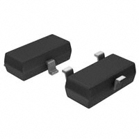
### 封装信息 ESDAxxL采用SOT23塑料封装,尺寸如下: - A:0.89mm至1.4mm(0.035至0.055英寸) - B:0.3mm至0.51mm(0.012至0.02英寸) - C:0.085mm至0.18mm(0.003至0.007英寸) - D:2.75mm至3.04mm(0.108至0.12英寸) - E:1.2mm至1.6mm(0.047至0.063英寸) - H:2.1mm至2.75mm(0.083至0.108英寸) - L:0.6mm(典型值) - S:0.35mm至0.65mm(0.014至0.026英寸)
ESDA5V3L 价格&库存

很抱歉,暂时无法提供与“ESDA5V3L”相匹配的价格&库存,您可以联系我们找货

免费人工找货
ESDA5V3L
  •  国内价格 香港价格
  • 3000+0.688753000+0.08826
  • 6000+0.621026000+0.07958
  • 9000+0.586489000+0.07516
  • 15000+0.5476415000+0.07018
  • 21000+0.5246321000+0.06723
  • 30000+0.5022630000+0.06436

库存:267798

ESDA5V3L
    •  国内价格
    • 10+2.16802
    • 50+2.10214
    • 100+2.06141
    • 250+2.02069
    • 1000+1.97996

    库存:720

    ESDA5V3L
      •  国内价格
      • 5+0.61701
      • 50+0.48177
      • 600+0.47454
      • 1200+0.46030

      库存:1150

      ESDA5V3L
      •  国内价格
      • 10+1.20500
      • 200+0.71880
      • 800+0.50310
      • 3000+0.35940
      • 6000+0.34140
      • 30000+0.31620

      库存:76315

      ESDA5V3L
      •  国内价格
      • 1+0.55440
      • 200+0.35750
      • 1500+0.31130
      • 3000+0.27500

      库存:76315