ESDAxxSCx
Quad Transil™ array for ESD protection
Features
■ ■ ■
4 unidirectional Transil Functions Low leakage current: IR max. < 20 µA at VRM 400 W peak pulse power (8/20 µs)
Benefits
■ ■ ■
High ESD protection level: up to 25 kV High integration Suitable for high density boards
SOT23-5L (SC-59) ESDAxxSC5
SOT23-6L (SC-59) ESDAxxSC6
Complies with the following standards:
■
Figure 1.
1 2 3
ESDAxxSC5 functional diagram
5
IEC 61000-4-2 level 4: – 15 kV (air discharge) – 8 kV (contact discharge) MIL STD 883E- Method 3015-7: class3B – human body model
■
4
Applications
Where transient overvoltage protection in ESD sensitive equipment is required, such as :
■ ■ ■ ■ ■ ■
Figure 2.
1 2 3
ESDAxxSC6 functional diagram
6 5 4
Computers Printers Communication systems Cellular phone handsets and accessories Other telephone set Set top boxes
Description
The ESDAxxSC5 and ESDAxxSC6 are monolithic voltage suppressors designed to protect components which are connected to data and transmission lines against ESD. They clamp the voltage just above the logic level supply for positive transients, and to a diode drop below ground for negative transient.
TM: Transil is a trademark of STMicroelectronics.
November 2007
Rev 9
1/11
www.st.com 11
�Characteristics
ESDAxxSCx
1
Table 1.
Symbol VPP
Characteristics
Absolute ratings (Tamb = 25 °C)
Parameter ESD discharge MIL STD 883E - Method 3015-7 IEC61000-4-2 air discharge IEC61000-4-2 contact discharge ESDA5V3SCx ESDA6V1SCx PPP Peak pulse power (8/20µs) ESDA14V2SCx ESDA17SC6 ESDA19SC6 ESDA25SC6 Value 25 500 400 Unit kV
W
300
W
Tj Tstg TL Top
Junction temperature Storage temperature range Maximum lead temperature for soldering during 10 s at 5mm for case Operating temperature range
150 -55 to +150 260 -40 to +125
°C °C °C °C
Table 2.
Symbol VRM VBR VCL IRM IPP αT C Rd VF
Electrical characteristics - definitions (Tamb = 25 °C)
Parameter
I IF
Stand-off voltage Breakdown voltage Clamping voltage Leakage current @ VRM Peak pulse current Voltage temperature coefficient Capacitance Dynamic resistance Forward voltage dropt
Rd
VBR VCL V RM VF I RM V
I PP
2/11
�ESDAxxSCx Table 3. Electrical characteristics - values (Tamb = 25 °C)
VBR @ IR Order codes min. V ESDA5V3SC5 ESDA5V3SC6 ESDA6V1SC5 ESDA6V1SC6 ESDA14V2SC5 ESDA14V2SC6 ESDA17SC6 ESDA19SC6 ESDA25SC6 5.3 6.1 14.2 17 19 25 max. V 5.9 7.2 15.8 19 21 30 mA 1 1 1 1 1 1 IRM @ VRM max. µA 2 20 5 0.075 0.1 1 V 3 5.25 12 14 15 24 Rd typ.(1) mΩ 230 350 650 700 800 1000
Characteristics
αT
max.(2) 10-4/C 5 6 10 10 8.5 10
C typ. 0 V bias pF 280 190 100 85 80 60
VF@ IF max. V 1.25 1.25 1.25 1.2 1.2 1.2 mA 200 200 200 10 10 10
1. Square pulse, Ipp = 15 A, tp=2.5 µs. 2. Δ VBR = αT* (Tamb -25 °C) * VBR (25 °C)
Figure 3.
Peak power dissipation versus initial junction temperature
Figure 4.
Peak pulse power versus exponential pulse duration (Tj initial = 25 °C)
PPP[Tj initial] / PPP[Tj initial=25°C]
1.1 1.0 0.9 0.8 0.7 0.6 0.5 0.4 0.3 0.2 0.1 0.0 0 25 50 75 100 125 150
PPP(W)
5000
ESDA5V3SC5/SC6 & ESDA6V1SC5/SC6
1000
ESDA14V2SC5/SC6 ESDA17SC6 ESDA19SC6 ESDA25SC6
Tj initial (°C)
100 1
tp(µs)
10 100
Figure 5.
Clamping voltage versus peak pulse current (Tj initial = 25 °C). Rectangular waveform tp = 2.5 µs
Figure 6.
Capacitance versus reverse applied voltage (typical values)
IPP(A)
50.0
ESDA25SC6 ESDA19SC6
C(pF)
500
F=1MHz VOSC=30mVRMS
ESDA5V3SC5/SC6
10.0
ESDA17SC6
ESDA14V2SC5/SC6 ESDA6V1SC5/SC6
100
ESDA6V1SC5/SC6
1.0
ESDA5V3SC5/SC6
ESDA14V2SC5/SC6 ESDA17SC6 ESDA19SC6
VCL(V)
0.1 0 5 10 15 20 25 30 35 40 45 50 55 60 65
tp=2.5µs
70
75
80
10 1 2 5
VR(V)
10 20
ESDA25SC6
50
3/11
�Application information
ESDAxxSCx
Figure 7.
Relative variation of leakage current versus junction temperature (typical values)
Figure 8.
Peak forward voltage drop versus peak forward current (typical values)
IR[Tj] / IR[Tj=25°C]
500
ESDA17SC6 & ESDA19SC6
5.00
IFM(A)
ESDA5V3SC5/SC6 ESDA14V2SC5/SC6 & ESDA6V1SC5/SC6 ESDA19SC6 ESDA17SC6
100
ESDA14V2SC5/SC6 & ESDA6V1SC5/SC6
1.00
ESDA25SC6
ESDA25SC6
10
0.10
Tj(°C)
1 25 50 75
ESDA5V3SC5/SC6
Tj = 25°C
VFM(V)
0.01
100 125
0.5
1.0
1.5
2.0
2.5
3.0
3.5
4.0
2
2.1
Application information
Calculation of the clamping voltage use of the dynamic resistance
The ESDA family has been designed to clamp fast spikes like ESD. Generally the PCB designers need to calculate easily the clamping voltage VCL. This is why we give the dynamic resistance in addition to the classical parameters. The voltage across the protection cell can be calculated with the following formula: VCL = VBR + Rd IPP Where IPP is the peak current through the ESDA cell. As the value of the dynamic resistance remains stable for a surge duration lower than 20 µs, the 2.5 µs rectangular surge is well adapted. In addition both rise and fall times are optimized to avoid any parasitic phenomenon during the measurement of Rd.
2.2
Dynamic resistance measurement
The short duration of the ESD has led us to prefer a more adapted test wave, as below defined, to the classical 8/20µs and 10/1000 µs surges. Figure 9. 2.5 µs duration measurement wave
I Ipp
2µs tp = 2.5µs
t
4/11
�ESDAxxSCx
Application information
2.3
ESD protection with ESDAxxSCx
Electrostatic discharge (ESD) is a major cause of failure in electronic systems. Transient Voltage Suppressors (TVS) are an ideal choice for ESD protection. They are capable of clamping the incoming transient overvoltage to a low enough level such that damage to the protected semiconductor is prevented. Surface mount TVS arrays offer the best choice for minimal lead inductance. They serve as parallel protection elements, connected between the signal line and ground. As the transient rises above the operating voltage of the device, the TVS array becomes a low impedance path diverting the transient current to ground. Figure 10. ESDAxxSCx array protection against ESD
I/ O LINES
ESD sensitive device
GND
ESDAxxxSC6 (1connection to GND for ESDAxxSC5)
The ESDAxxSCx array is the ideal board level protection of ESD sensitive semiconductor components. The tiny SOT23-5L and SOT23-6L packages allow design flexibility in the high density boards where the space saving is at a premium. This enables to shorten the routing and contributes to hardening against ESD.
2.4
Advice for optimizing circuit board layout
Circuit board layout is a critical design step in the suppression of ESD induced transients. The following guidelines are recommended:
● ● ● ● ●
The ESDAxxSC5/6 should be placed as close as possible to the input terminals or connectors. The path length between the ESD suppressor and the protected line should be minimized All conductive loops, including power and ground loops should be minimized The ESD transient return path to ground should be kept as short as possible Ground planes should be used whenever possible
5/11
�Technical information
ESDAxxSCx
3
3.1
Technical information
ESD protection
The ESDA19SC6 is particularly optimized to perform ESD protection. ESD protection is achieved by clamping the unwanted overvoltage. The clamping voltage is given by the following formula : VCL = VBR + Rd . IPP As shown in Figure 11., the ESD strikes are clamped by the transient voltage suppressor. Figure 11. ESD clamping behavior (example)
Rg
Rd
Vg
VBR
Voutput
Rload
Device to be protected
ESD Surge
ESDA19SC6
To have a good approximation of the remaining voltages at both VI/O side, we provide the typical dynamical resistance value Rd. By taking into account the following hypothesis : Rg > Rd and Rload > Rd we have:
Vg V output = V BR + R d × -----Rg
The results of the calculation done for Vg = 8 kV, Rg = 330 Ω (IEC61000-4-2 standard), VBR = 19 V (typ.) and Rd = 0.80 Ω (typ.) give: Vouput = 38.4 V This confirms the very low remaining voltage across the device to be protected. It is also important to note that in this approximation the parasitic inductance effect was not taken into account. This could be a few tenths of volts during a few nanoseconds at the output side.
6/11
�ESDAxxSCx
Ordering information
4
Ordering information
Figure 12. Ordering information scheme
ESDA
ESD Array Breakdown Voltage (min) 5V3 = 5.3 Volt 6V1 = 6.1 Volt 14V2 = 14.2 Volt 17 = 17 Volt 19 = 19 Volt 25 = 25 Volt Package SC5 = SOT23-5L SC6 = SOT23-6L
xx
SCx
7/11
�Package information
ESDAxxSCx
5
Package information
●
Epoxy meets UL94, V0 standard
In order to meet environmental requirements, ST (also) offers these devices in ECOPACK® packages. ECOPACK® packages are Lead-free. The category of second level Interconnect is marked on the inner box label, in compliance with JEDEC Standard JESD97. The maximum ratings related to soldering conditions are also marked on the inner box label. ECOPACK is an ST trademark. ECOPACK specifications are available at: www.st.com. Table 4. SOT23-5L dimensions
Dimensions Ref.
A E
Millimeters Min. Typ. Max. Min.
Inches Typ. Max. 0.057 0.004 0.051 0.020 0.008 0.118 0.069 0.037
A
e B e D
0.90 0 0.90 0.35 0.09 2.80 1.50 0.95 2.60 0.10 0°
1.45 0.035 0.10 0
A1 A2 b c
A2
1.30 0.035 0.50 0.014 0.20 0.004 3.05 0.11
D E e
1.75 0.059
c
A1
θ
L H
H L M
3.00 0.102 0.60 0.004 10° 0°
0.118 0.024 10°
Figure 13. SOT23-5L footprint (dimensions in mm)
0.60
1.20
0.95 3.50 2.30 1.10
8/11
�ESDAxxSCx Table 5. SOT23-6L dimensions
Package information
Dimensions Ref.
A E
Millimeters Min. Typ. Max. Min.
Inches Typ. Max. 0.057 0.004 0.051 0.020 0.008 0.118 0.069 0.037
A
e b e D
0.90 0 0.90 0.35 0.09 2.80 1.50 0.95 2.60 0.10 0°
1.45 0.035 0.10 0
A1 A2 b c
A2
1.30 0.035 0.50 0.014 0.20 0.004 3.05 0.11
D E e
1.75 0.059
c
A1
θ
L H
H L θ
3.00 0.102 0.60 0.004 10° 0°
0.118 0.024 10°
Figure 14. SOT23-6L footprint (dimensions in mm)
0.60
1.20
0.95 3.50 2.30 1.10
9/11
�Ordering information
ESDAxxSCx
6
Ordering information
Table 6. Ordering information
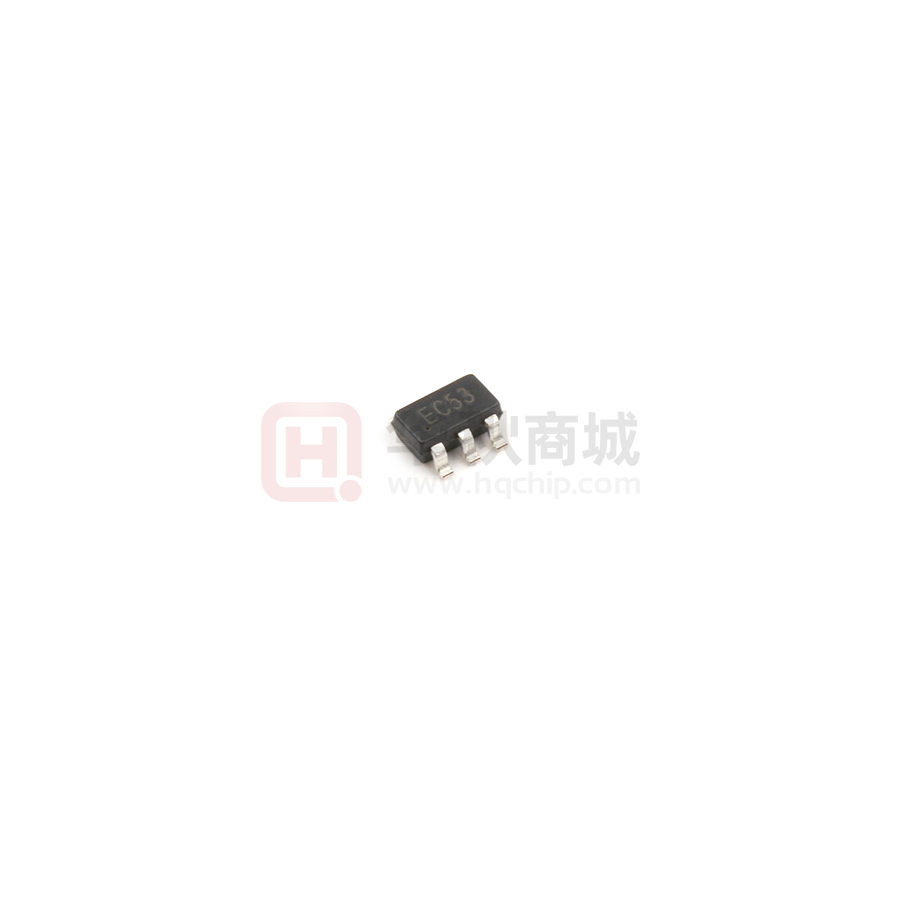
Marking EC53 EC61 EC15 ES53 ES61 ES15 SOT23-6L ESDA17SC6 ESDA19SC6 ESDA25SC6 ES17 ES19 ES25 16.7 mg 3000 Tape and reel SOT23-5L Package Weight Base qty Delivery mode
Order codes ESDA5V3SC5 ESDA6V1SC5 ESDA14V2SC5 ESDA5V3SC6 ESDA6V1SC6 ESDA14V2SC6
7
Revision history
Table 7.
Date Nov-2003 4-Nov-2004
Document revision history
Revision 7F 8 Previous issue. SOT23-6L package dimensions change for reference “D” from 3.0 millimeters (0.118 inches) to 3.05 millimeters (0.120 inches). Reformatted to current standard. Units for IRM MAX inTable 3 corrected to µA. Ordering information scheme expanded to cover all devices. Package information for SOT23-5L updated. Description of changes
22-Nov-2007
9
10/11
�ESDAxxSCx
Please Read Carefully:
Information in this document is provided solely in connection with ST products. STMicroelectronics NV and its subsidiaries (“ST”) reserve the right to make changes, corrections, modifications or improvements, to this document, and the products and services described herein at any time, without notice. All ST products are sold pursuant to ST’s terms and conditions of sale. Purchasers are solely responsible for the choice, selection and use of the ST products and services described herein, and ST assumes no liability whatsoever relating to the choice, selection or use of the ST products and services described herein. No license, express or implied, by estoppel or otherwise, to any intellectual property rights is granted under this document. If any part of this document refers to any third party products or services it shall not be deemed a license grant by ST for the use of such third party products or services, or any intellectual property contained therein or considered as a warranty covering the use in any manner whatsoever of such third party products or services or any intellectual property contained therein.
UNLESS OTHERWISE SET FORTH IN ST’S TERMS AND CONDITIONS OF SALE ST DISCLAIMS ANY EXPRESS OR IMPLIED WARRANTY WITH RESPECT TO THE USE AND/OR SALE OF ST PRODUCTS INCLUDING WITHOUT LIMITATION IMPLIED WARRANTIES OF MERCHANTABILITY, FITNESS FOR A PARTICULAR PURPOSE (AND THEIR EQUIVALENTS UNDER THE LAWS OF ANY JURISDICTION), OR INFRINGEMENT OF ANY PATENT, COPYRIGHT OR OTHER INTELLECTUAL PROPERTY RIGHT. UNLESS EXPRESSLY APPROVED IN WRITING BY AN AUTHORIZED ST REPRESENTATIVE, ST PRODUCTS ARE NOT RECOMMENDED, AUTHORIZED OR WARRANTED FOR USE IN MILITARY, AIR CRAFT, SPACE, LIFE SAVING, OR LIFE SUSTAINING APPLICATIONS, NOR IN PRODUCTS OR SYSTEMS WHERE FAILURE OR MALFUNCTION MAY RESULT IN PERSONAL INJURY, DEATH, OR SEVERE PROPERTY OR ENVIRONMENTAL DAMAGE. ST PRODUCTS WHICH ARE NOT SPECIFIED AS "AUTOMOTIVE GRADE" MAY ONLY BE USED IN AUTOMOTIVE APPLICATIONS AT USER’S OWN RISK.
Resale of ST products with provisions different from the statements and/or technical features set forth in this document shall immediately void any warranty granted by ST for the ST product or service described herein and shall not create or extend in any manner whatsoever, any liability of ST.
ST and the ST logo are trademarks or registered trademarks of ST in various countries. Information in this document supersedes and replaces all information previously supplied. The ST logo is a registered trademark of STMicroelectronics. All other names are the property of their respective owners.
© 2007 STMicroelectronics - All rights reserved STMicroelectronics group of companies Australia - Belgium - Brazil - Canada - China - Czech Republic - Finland - France - Germany - Hong Kong - India - Israel - Italy - Japan Malaysia - Malta - Morocco - Singapore - Spain - Sweden - Switzerland - United Kingdom - United States of America www.st.com
11/11
�
很抱歉,暂时无法提供与“ESDA5V3SC5”相匹配的价格&库存,您可以联系我们找货
免费人工找货- 国内价格
- 1+0.48412
- 10+0.44411
- 30+0.43611
- 100+0.41210


 工商网监
湘ICP备2023018690号
工商网监
湘ICP备2023018690号
