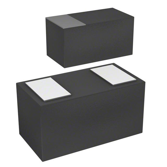
ESDU401-1BF4
Datasheet
40 V single line ESD protection with ultra-low capacitance
Features
0201 package
•
•
•
•
•
Ultra Low capacitance : 1 pF
Bidirectional device
High working voltage : 40 V
Low leakage current : 50 nA max.
0201 package size compatible
•
•
Ultra small PCB area: 0.18 mm2
Low clamping voltage: 105 V at 16 A Ipp TLP
•
•
Halogen free and RoHS compliant component
Exceeds IEC 61000-4-2 level 4 standard:
–
±16 kV (air discharge)
–
±9.5 kV (contact discharge)
Application
Product status link
ESDU401-1BF4
Where transient over voltage protection in ESD sensitive equipment is required, such
as:
•
Smartphones, mobile phones and accessories
•
Tablets and notebooks
•
Portable multimedia devices and accessories
•
Wearable, home automation, healthcare
•
Highly integrated systems
Description
The ESDU401-1BF4 is high voltage, ultra low capacitance bidirectional single line
TVS diode designed to protect the data line or other I/O ports against ESD transients.
The device is ideal for all applications where both reduced line capacitance and
board space saving are required.
DS13060 - Rev 1 - September 2019
For further information contact your local STMicroelectronics sales office.
www.st.com
�ESDU401-1BF4
Characteristics
1
Characteristics
Table 1. Absolute maximum ratings (Tamb = 25 °C)
Symbol
Parameter
Value
IEC 61000-4-2 contact discharge
±9.5
IEC 61000-4-2 air discharge
±16
Unit
Vpp
Peak pulse voltage
Ppp
Peak pulse power (8/20 μs)
40
W
Ipp
Peak pulse current (8/20 μs)
0.7
A
Tj
Operating junction temperature range
-55 to +150
Storage junction temperature range
-65 to +150
Tstg
TL
Maximum lead temperature for soldering during 10 s
kV
°C
260
Figure 1. Electrical characteristics (definitions)
I
IPP
=
=
=
=
=
Parameter
Breakdown voltage at IR
Clamping voltage
Leakage current at VRM
Stand-off voltage
Peak pulse current at VCL
IR
=
=
Dynamic resistance
Current for VBR measurement
C LINE
=
Input capacitance per line
Symbol
VBR
VCL
IRM
VRM
IPP
RD
VCL VBR VRM
IR
IRM
V
IRM
IR
V RM VBR VCL
IPP
Table 2. Electrical characteristics (values) (Tamb = 25° C)
Symbol
VBR
IR = 1 mA
IRM
Leakage current
VCL
Clamping voltage
VCL
Clamping voltage
RD
CLINE
DS13060 - Rev 1
Parameter
Test condition
Min.
Typ.
Max.
Unit
41
44
46
V
50
nA
VRM = 40 V
IEC 61000-4-2, 8 kV
105
V
8/20 µs waveform, IPP = 0.7 A
50
V
Dynamic resistance
Pulse duration 100 ns
3.5
Ω
Line capacitance
VLINE = 40 V, F = 1 MHz, VOSC = 30 mV
1.1
contact discharge measured after 30 ns
1.3
pF
page 2/10
�ESDU401-1BF4
Characteristics (curves)
1.1
Characteristics (curves)
Figure 2. Leakage current versus junction temperature
(typical values)
Figure 3. Junction capacitance versus applied voltage
(typical values)
Figure 4. ESD response to IEC 61000-4-2
(+8 kV contact discharge)
Figure 5. ESD response to IEC 61000-4-2
(-8 kV contact discharge)
20 V/div
20 V/div
1
2
3
4
105 V
1
88 V
2
81 V
3
Peak clamping voltage
Clamping voltage at 30 ns
Clamping voltage at 60 ns
Clamping voltage at 100 ns
63V
4
4
1
-104 V
2
-84 V
3
-81 V
20 ns/div
62 V
1
2
3
4
Peak clamping voltage
Clamping voltage at 30 ns
Clamping voltage at 60 ns
Clamping voltage at 100 ns
20 ns/div
Figure 6. S21 attenuation measurement result
S21(dB)
F(Hz)
DS13060 - Rev 1
page 3/10
�ESDU401-1BF4
Package information
2
Package information
In order to meet environmental requirements, ST offers these devices in different grades of ECOPACK packages,
depending on their level of environmental compliance. ECOPACK specifications, grade definitions and product
status are available at: www.st.com. ECOPACK is an ST trademark.
2.1
ST0201 package information
Figure 7. ST0201 package outline
Table 3. ST0201 package mechanical data
Dimensions
Millimeters
Ref.
Min.
Typ.
Max.
Min.
Typ.
Max.
A
0.280
0.300
0.320
0.0110
0.0118
0.0126
b
0.125
0.140
0.155
0.0049
0.0055
0.0061
D
0.570
0.600
0.630
0.0224
0.0236
0.0248
D1
Note:
DS13060 - Rev 1
Inches
0.350
0.0138
E
0.270
0.300
0.330
0.0106
0.0118
0.0130
E1
0.175
0.190
0.205
0.0069
0.0075
0.0081
fD
0.040
0.055
0.070
0.0015
0.0021
0.0028
fE
0.040
0.055
0.070
0.0115
0.0021
0.0028
Marking can be rotated by 90° or 180° to differentiate assembly location.
page 4/10
�ESDU401-1BF4
ST0201 package information
Figure 8. Tape and reel specification
Bar indicates Pin 1
DS13060 - Rev 1
page 5/10
�ESDU401-1BF4
Recommendation on PCB assembly
3
Recommendation on PCB assembly
3.1
Footprint
1.
Footprint in mm
a.
SMD footprint design is recommended.
Figure 9. Footprint in mm
0.150
0.225
0.187
Solder mask opening
3.2
Stencil opening design
1.
Reference design
a.
Stencil opening thickness: 75 μm / 3 mils
Figure 10. Recommended stencil window position in mm
0.167
0.210
0.170
Stencil apertures
DS13060 - Rev 1
page 6/10
�ESDU401-1BF4
Solder paste
3.3
Solder paste
1.
2.
3.
4.
3.4
Placement
1.
2.
3.
4.
5.
6.
3.5
Manual positioning is not recommended.
It is recommended to use the lead recognition capabilities of the placement system, not the outline centering
Standard tolerance of ±0.05 mm is recommended.
1.0 N placement force is recommended. Too much placement force can lead to squeezed out solder paste
and cause solder joints to short. Too low placement force can lead to insufficient contact between package
and solder paste that could cause open solder joints or badly centered packages.
To improve the package placement accuracy, a bottom side optical control should be performed with a high
resolution tool.
For assembly, a perfect supporting of the PCB (all the more on flexible PCB) is recommended during solder
paste printing, pick and place and reflow soldering by using optimized tools.
PCB design preference
1.
2.
3.6
Halide-free flux qualification ROL0 according to ANSI/J-STD-004.
“No clean” solder paste is recommended.
Offers a high tack force to resist component movement during high speed.
Use solder paste with fine particles: powder particle size 20-38 µm.
To control the solder paste amount, the closed via is recommended instead of open vias.
The position of tracks and open vias in the solder area should be well balanced. A symmetrical layout is
recommended, to avoid any tilt phenomena caused by asymmetrical solder paste due to solder flow away.
Reflow profile
Figure 11. ST ECOPACK recommended soldering reflow profile for PCB mounting
250
240-245 °C
Temperature (°C)
-2 °C/s
2 - 3 °C/s
60 sec
(90 max)
200
-3 °C/s
150
-6 °C/s
100
0.9 °C/s
50
Time (s)
0
Note:
DS13060 - Rev 1
30
60
90
120
150
180
210
240
270
300
Minimize air convection currents in the reflow oven to avoid component movement. Maximum soldering profile
corresponds to the latest IPC/JEDEC J-STD-020.
page 7/10
�ESDU401-1BF4
Ordering information
4
Ordering information
Table 4. Ordering information
Order code
Marking
Package
Weight
Base qty.
Delivery mode
ESDU401-1BF4
9(1)
ST0201
0.116 mg
15000
Tape and reel
1. The marking can be rotated by multiples of 90° to differentiate assembly location
DS13060 - Rev 1
page 8/10
�ESDU401-1BF4
Revision history
Table 5. Document revision history
DS13060 - Rev 1
Date
Revision
30-Sep-2019
1
Changes
First issue.
page 9/10
�ESDU401-1BF4
IMPORTANT NOTICE – PLEASE READ CAREFULLY
STMicroelectronics NV and its subsidiaries (“ST”) reserve the right to make changes, corrections, enhancements, modifications, and improvements to ST
products and/or to this document at any time without notice. Purchasers should obtain the latest relevant information on ST products before placing orders. ST
products are sold pursuant to ST’s terms and conditions of sale in place at the time of order acknowledgement.
Purchasers are solely responsible for the choice, selection, and use of ST products and ST assumes no liability for application assistance or the design of
Purchasers’ products.
No license, express or implied, to any intellectual property right is granted by ST herein.
Resale of ST products with provisions different from the information set forth herein shall void any warranty granted by ST for such product.
ST and the ST logo are trademarks of ST. For additional information about ST trademarks, please refer to www.st.com/trademarks. All other product or service
names are the property of their respective owners.
Information in this document supersedes and replaces information previously supplied in any prior versions of this document.
© 2019 STMicroelectronics – All rights reserved
DS13060 - Rev 1
page 10/10
�
很抱歉,暂时无法提供与“ESDU401-1BF4”相匹配的价格&库存,您可以联系我们找货
免费人工找货- 国内价格 香港价格
- 1+3.814271+0.47326
- 10+2.6874310+0.33345
- 100+1.35810100+0.16851
- 500+1.10813500+0.13750
- 1000+0.822231000+0.10202
- 2000+0.691742000+0.08583
- 5000+0.661355000+0.08206
- 国内价格 香港价格
- 15000+0.5578815000+0.06922
- 30000+0.5125330000+0.06360
- 45000+0.4894145000+0.06073
- 75000+0.4634075000+0.05750
- 105000+0.44800105000+0.05559
- 150000+0.44243150000+0.05490


 工商网监
湘ICP备2023018690号
工商网监
湘ICP备2023018690号
