ESM2012DV
®
NPN DARLINGTON POWER MODULE
■
■
■
■
■
■
■
HIGH CURRENT POWER BIPOLAR MODULE
VERY LOW Rth JUNCTION TO CASE
SPECIFIED ACCIDENTAL OVERLOAD
AREAS
ULTRAFAST FREEWHEELING DIODE
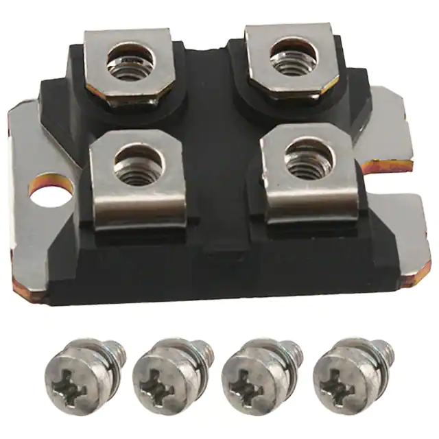
FULLY INSULATED PACKAGE (UL
COMPLIANT)
EASY TO MOUNT
LOW INTERNAL PARASITIC INDUCTANCE
)
s
(
ct
u
d
o
r
P
e
INDUSTRIAL APPLICATIONS:
MOTOR CONTROL
■ UPS
■ DC/DC & DC/AC CONVERTERS
■
t
e
l
o
)
(s
s
b
O
ISOTOP
INTERNAL SCHEMATIC DIAGRAM
t
c
u
d
o
r
P
e
t
e
l
o
s
b
O
ABSOLUTE MAXIMUM RATINGS
Symbol
V CEV
Parameter
Collector-Emitter Voltage (V BE = -5 V)
V CEO(sus) Collector-Emitter Voltage (I B = 0)
V EBO
IC
I CM
Emitter-Base Voltage (I C = 0)
Value
Unit
150
V
120
V
7
V
Collector Current
120
A
Collector Peak Current (t p = 10 ms)
180
A
A
Base Current
2
I BM
Base Peak Current (t p = 10 ms)
4
A
P tot
Total Dissipation at T c = 25 o C
175
W
V isol
Insulation Withstand Voltage (RMS) from All
Four Terminals to Exernal Heatsink
Storage Temperature
2500
V
IB
T stg
Tj
Max. Operating Junction Temperature
September 2003
-55 to 150
o
C
150
o
C
1/8
�ESM2012DV
THERMAL DATA
R thj-case
R thj-case
R thc-h
Thermal Resistance Junction-case (transistor)
Thermal Resistance Junction-case (diode)
Thermal Resistance Case-heatsink With Conductive
Grease Applied
Max
Max
0.7
0.9
o
Max
0.05
o
o
C/W
C/W
C/W
ELECTRICAL CHARACTERISTICS (Tcase = 25 oC unless otherwise specified)
Symbol
Parameter
Test Conditions
I CER #
Collector Cut-off
Current (R BE = 5 Ω)
V CE = V CEV
V CE = V CEV
T j = 100 o C
I CEV #
Collector Cut-off
Current (V BE = -5V)
V CE = V CEV
V CE = V CEV
T j = 100 o C
I EBO #
Emitter Cut-off Current
(I C = 0)
V EB = 5 V
V CEO(SUS) * Collector-Emitter
Sustaining Voltage
(I B = 0)
IC = 5 A
L = 15 mH
V clamp = 125 V
h FE ∗
V CE(sat) ∗
V BE(sat) ∗
DC Current Gain
I C = 100 A
Collector-Emitter
Saturation Voltage
IC
IC
IC
IC
=
=
=
=
70 A
70 A
100 A
100 A
=
=
=
=
bs
O
)
I C = 100 A
I C = 100 A
IB = 1 A
IB = 1 A
di C /dt
Rate of Rise of
On-state Collector
V CC = 90 V
I B1 = 0.5 A
RC = 0
tp = 3 µs
T j = 100 o C
V CE (3
µs)••
Collector-Emitter
Dynamic Voltage
V CE (5
µs)••
Collector-Emitter
Dynamic Voltage
u
d
o
s
(
t
c
e
t
e
ol
mA
mA
1
7
mA
mA
1
mA
V
1200
1.25
1.35
1.5
1.65
2
V
V
V
V
3
V
V
1.5
230
A/µs
R C = 1.3 Ω
T j = 100 o C
2
3
V
V CC = 90 V
I B1 = 0.5 A
R C = 1.3 Ω
T j = 100 o C
1.8
2.5
V
0.9
0.15
0.3
2
0.3
0.6
µs
µs
µs
V CC = 90 V
R BB = Ω
I B1 = 0.25 A
o
T j = 100 C
Maximum Collector
Emitter Voltage
Without Snubber
I CWoff = 120 A
V BB = -5 V
L = 60 µH
T j = 125 o C
I B1 = 1A
V CC = 90 V
R BB = 1.25 Ω
VF∗
Diode Forward Voltage
I F = 100 A
I RM
Reverse Recovery
Current
V CC = 125 V
I F = 100 A
di F /dt = -200 A/µs L < 0.05 µH
T j = 100 o C
V CEW
1.5
10
V CC = 90 V
I B1 = 0.5 A
I C = 70 A
V BB = -5 V
V clamp = 125 V
L = 60 µH
s
b
O
200
Unit
)
s
(
ct
2.3
2.35
T j = 100 o C
Storage Time
Fall Time
Cross-over Time
ts
tf
tc
T j = 100 o C
∗ Pulsed: Pulse duration = 300 µs, duty cycle 1.5 %
# See test circuits in databook introduction
To evaluate the conduction losses of the diode use the following equations:
P = 0.66 IF(AV) + 0.0034 I2F(RMS)
VF = 0.66 + 0.0034 IF
2/8
t
e
l
o
0.25 A
0.25 A T j = 100 o C
1A
1 A T j = 100 o C
Max.
u
d
o
r
P
e
V CE = 5 V
IB
IB
IB
IB
Typ.
125
Base-Emitter
Saturation Voltage
Pr
Min.
125
V
0.92
1
V
10
14
A
�ESM2012DV
Safe Operating Areas
Thermal Impedance
)
s
(
ct
u
d
o
r
P
e
Derating Curve
Collector-emitter Voltage Versus
base-emitter Resistance
t
e
l
o
)
(s
s
b
O
t
c
u
d
o
r
P
e
s
b
O
t
e
l
o
Collector Emitter Saturation Voltage
Base-Emitter Saturation Voltage
3/8
�ESM2012DV
Reverse Biased SOA
Foward Biased SOA
)
s
(
ct
u
d
o
r
P
e
Reverse Biased AOA
Forward Biased AOA
t
e
l
o
)
(s
s
b
O
t
c
u
d
o
r
P
e
t
e
l
o
s
b
O
Switching Times Inductive Load
4/8
Switching Times Inductive Load Versus
Temperature
�ESM2012DV
Typical VF Versus IF
Dc Current Gain
)
s
(
ct
u
d
o
r
P
e
Peak Reverse Current Versus diF/dt
Turn-on Switching Test Circuit
t
e
l
o
)
(s
s
b
O
t
c
u
d
o
r
P
e
t
e
l
o
s
b
O
Turn-on Switching Waveforms
5/8
�ESM2012DV
Turn-on Switching Test Circuit
Turn-off Switching Waveforms
)
s
(
ct
u
d
o
r
P
e
Turn-off Switching Test Circuit of Diode
Turn-off Switching Waveform of Diode
t
e
l
o
)
(s
t
c
u
d
o
r
P
e
t
e
l
o
s
b
O
6/8
s
b
O
�ESM2012DV
ISOTOP MECHANICAL DATA
mm
DIM.
MIN.
inch
TYP.
MAX.
MIN.
TYP.
MAX.
A
11.8
12.2
0.465
0.480
A1
8.9
9.1
0.350
0.358
B
7.8
8.2
0.307
0.322
C
0.75
0.85
0.029
0.033
C2
1.95
2.05
0.076
0.080
D
37.8
38.2
1.488
D1
31.5
31.7
1.240
E
25.15
25.5
0.990
E1
23.85
24.15
0.938
0.586
E2
24.8
14.9
15.1
G1
12.6
12.8
G2
3.5
4.3
F
4.1
4.3
F1
4.6
5
P
4
4.3
4
S
30.1
1.248
Pr
u
d
o
1.003
0.950
0.976
G
P1
)
s
(
ct
1.503
bs
O
)
4.4
s
(
t
c
30.3
e
t
e
ol
0.496
0.594
0.503
0.137
1.169
0.161
0.169
0.181
0.196
0.157
0.169
0.157
0.173
1.185
1.193
u
d
o
r
P
e
t
e
l
o
s
b
O
P093A
7/8
�ESM2012DV
)
s
(
ct
u
d
o
r
P
e
t
e
l
o
)
(s
s
b
O
t
c
u
d
o
r
P
e
t
e
l
o
s
b
O
Information furnished is believed to be accurate and reliable. However, STMicroelectronics assumes no responsibility for the consequences
of use of such information nor for any infringement of patents or other rights of third parties which may result from its use. No license is
granted by implication or otherwise under any patent or patent rights of STMicroelectronics. Specification mentioned in this publication are
subject to change without notice. This publication supersedes and replaces all information previously supplied. STMicroelectronics products
are not authorized for use as critical components in life support devices or systems without express written approval of STMicroelectronics.
The ST logo is a trademark of STMicroelectronics.
All other names are the property of their respective owners.
© 2003 STMicroelectronics – All Rights reserved
STMicroelectronics GROUP OF COMPANIES
Australia - Belgium - Brazil - Canada - China - Czech Republic - Finland - France - Germany - Hong Kong - India - Israel - Italy - Japan Malaysia - Malta - Morocco - Singapore - Spain - Sweden - Switzerland - United Kingdom - United States.
http://www.st.com
8/8
�
很抱歉,暂时无法提供与“ESM2012DV”相匹配的价格&库存,您可以联系我们找货
免费人工找货