EV-VND7030AJ
VND7030AJ evaluation board
Data brief
Features
Max transient supply voltage
VCC
40 V
Operating voltage range
VCC
4 to 28 V
Typ. on-state resistance (per Ch)
RON
31 mΩ
Current limitation (typ)
ILIMH
56 A
Stand-by current (max)
ISTBY
0.5 µA
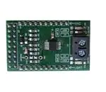
Simple single IC application board dedicated
for VND7030AJ
Provides electrical connectivity and thermal
heat-sinking for easy prototyping
General device features
Double channel smart high-side driver
with MultiSense analog feedback
Very low standby current
Compatible with 3 V and 5 V CMOS
outputs
September 2015
Diagnostic functions
Multiplexed analog feedback of: load
current with high precision proportional
current mirror, VCC supply voltage and
TCHIP device temperature
Overload and short to ground (power
limitation) indication
Thermal shutdown indication
OFF-state open-load detection
Output short to VCC detection
Sense enable/disable
Protections
Undervoltage shutdown
Overvoltage clamp
Load current limitation
Self limiting of fast thermal transients
Configurable latch-off on
overtemperature or power limitation
with dedicated fault reset pin
Loss of ground and loss of VCC
Reverse battery with external
components
Electrostatic discharge protection
Applications
Typical applications are all types of automotive
resistive, inductive and capacitive loads.
Table 1: Device summary
Order code
EV-VND7030AJ
DocID026359 Rev 3
Reference
VND7030AJ evaluation board
1/7
www.st.com
�Description
1
EV-VND7030AJ
Description
®
®
This board provides you an easy way to connect STMicroelectronics VIPower M0-7
technology into your existing system.
The board comes pre-assembled with VND7030AJ high-side driver. On board minimum set
of electrical components (as for device datasheet recommendation) is enabling the user to
directly connect the load, the power supply and the microcontroller without any additional
effort in external component design and connection.
The VND7030AJ is a double channel high-side driver manufactured using ST proprietary
VIPower technology and housed in PowerSSO-16 package. The device is designed to
drive 12 V automotive grounded loads through a 3 V and 5 V CMOS-compatible interface
and to provide protection and diagnostics.
The device integrates advanced protective functions such as load current limitation,
overload active management by power limitation and overtemperature shutdown with
configurable latch-off.
A FaultRST pin unlatches the output in case of fault or disables the latch-off functionality.
A dedicated multifunction multiplexed analog output pin delivers sophisticated diagnostic
functions including high precision proportional load current sense, supply voltage feedback
and chip temperature sense, in addition to the detection of overload and short circuit to
ground, short to VCC and OFF-state open-load. A sense enable pin allows OFF-state
diagnosis to be disabled during the module low-power mode as well as external sense
resistor sharing among similar devices.
Figure 1: Evaluation board schematic
Vbat
Vbat
J1
1
2
3
4
5
6
7
8
9
10
C1
100nF
In_PullU P
0
R_UP1
J3
In_PullU P
FaultRS T
MultiSense
S_EN
SEL0
SEL1
IN0
IN1
+5V
1
2
3
4
5
6
7
8
9
10
11
12
13
14
15
16
17
18
IN0
IN1
R1 15K
R2 15K
FaultRS T
MultiSense
S_EN
R5 15K
C3
10nF
1
Rsense
TP1
SEL0
SEL1
PGND
R4 15K
R6 15K
R7 15K
1
PGND
1
8
R3 15K
TP2
2
3
7
5
6
4
INPUT0
INPUT1
FaultRS T
SEn
MultiSense
SEL0
SEL1
J2
R_UP2
1
VB ATT
U1
OUTPUT0
OUTPUT0
OUTPUT0
OUTPUT0
OUTPUT1
OUTPUT1
OUTPUT1
OUTPUT1
16
15
14
13
2
PGND
Vbat
Out0
12
11
10
9
Out1
GND
PSS0-16
D1
R8
4K7
ES1D L
CON18
PGND
LED1
LED2
C2
10n F
1
2
3
4
5
6
7
8
9
10
C4
10n F
R9
2k2
PGND
R10
2k2
J4
PGND
PGND
GAPG1704141132CFT
2/7
DocID026359 Rev 3
�EV-VND7030AJ
2
Board connections
Board connections
Figure 2: "Evaluation board connections" shows the placement of the connectors to be
used for supplying the evaluation board, connecting the load and controlling the
functionality and diagnostic of the device.
Figure 2: Evaluation board connections
Table 2: J3 connector: pin functions
Connector
Pin
number
Pin name
J3
1…4
N/A
J3
5
IN_PullUP
J3
6
+5V
J3
7
FaultRST
Active low compatible with 3 V and 5 V CMOS outputs pin; it
unlatches the output in case of fault; If kept low, sets the
outputs in auto-restart
J3
8
MultiSense
Multiplexed analog sense output pin; it delivers a current
proportional to the selected diagnostic: load current, supply
voltage or chip temperature
J3
9
S_EN
Active high compatible with 3 V and 5 V CMOS outputs pin;
it enables the MultiSense diagnostic pin.
J3
10
SEL0
Active high compatible with 3 V and 5 V CMOS outputs pin;
together with SEL1, it addresses the MultiSense multiplexer
J3
11
SEL1
Active high compatible with 3 V and 5 V CMOS outputs pin;
together with SEL0, it addresses the MultiSense multiplexer
J3
12
N/A
Not connected
J3
13
IN0
Voltage controlled input pin with hysteresis, compatible with
3 V and 5 V CMOS outputs. It controls OUT0 switch state
J3
14
IN1
Voltage controlled input pin with hysteresis, compatible with
3 V and 5 V CMOS outputs. It controls OUT1 switch state
J3
15…18
N/A
Not connected
Pin function
Not connected
Connection to optional external pull-up resistor for open load
detection in off-state.
5 V Power Supply
DocID026359 Rev 3
3/7
�Board connections
EV-VND7030AJ
In case the user wishes to utilize the Current Sense/MultiSense function of the device, it is
necessary to plug a sense resistor in RSENSE.
The package includes a through-hole resistor, to be mounted on TP1-TP2 (see Figure 4:
"Mounting through-hole sense resistor").
Different RSENSE values can be adopted based on user preference.
Another option is soldering an SMD resistor on the dedicated PCB pad, as shown in Figure
5: "Pads for soldering SMD resistor".
Figure 3: No sense resistor
Figure 4: Mounting through-hole sense resistor
Figure 5: Pads for soldering SMD resistor
4/7
DocID026359 Rev 3
�EV-VND7030AJ
3
Thermal data
Thermal data
Table 3: Thermal data
Symbol
Rthj-amb
Parameter
Thermal resistance junction-ambient (MAX)
Max
Unit
39
°C/W
Table 4: PCB specifications
Parameter
Value
Board dimensions
25 mm x 41.5 mm
Number of Cu layer
2
Layer Cu thickness
35 μm
Board finish thickness
1.6 mm +/- 10%
Board Material
FR4
Thermal vias separation
1.1 mm
Thermal vias diameter
0.5 mm
DocID026359 Rev 3
5/7
�Revision history
4
EV-VND7030AJ
Revision history
Table 5: Revision history
6/7
Date
Revis
ion
15-May-2014
1
Initial release.
21-Jul-2014
2
Updated Figure 1: "Evaluation board schematic"
01-Sep-2015
3
Changed EV-VND7030AJ-E in EV-VND7030AJ. Updated Section
"Features" and Section 1: "Description"
Changes
DocID026359 Rev 3
�EV-VND7030AJ
IMPORTANT NOTICE – PLEASE READ CAREFULLY
STMicroelectronics NV and its subsidiaries (“ST”) reserve the right to make changes, corrections, enhancements, modifications, and
improvements to ST products and/or to this document at any time without notice. Purchasers should obtain the latest relevant information on ST
products before placing orders. ST products are sold pursuant to ST’s terms and conditions of sale in place at the time of order
acknowledgement.
Purchasers are solely responsible for the choice, selection, and use of ST products and ST assumes no liability for application assistance or the
design of Purchasers’ products.
No license, express or implied, to any intellectual property right is granted by ST herein.
Resale of ST products with provisions different from the information set forth herein shall void any warranty granted by ST for such product.
ST and the ST logo are trademarks of ST. All other product or service names are the property of their respective owners.
Information in this document supersedes and replaces information previously supplied in any prior versions of this document.
© 2015 STMicroelectronics – All rights reserved
DocID026359 Rev 3
7/7
�
很抱歉,暂时无法提供与“EV-VND7030AJ”相匹配的价格&库存,您可以联系我们找货
免费人工找货