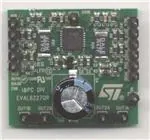
EVAL6227QR
Demonstration board mounting the L6227Q dual full-bridge driver
Data brief
Features
■
Operating supply voltage from 8 to 52 V
■
2.8 A output peak current (1.4 A DC)
■
RDS(on) 0.73 Ω typ. value @ TJ = 25 °C
■
Operating frequency up to 100 kHz
■
Non dissipative overcurrent protection
■
Dual independent constant tOFF PWM current
controllers
■
Slow decay synchronous rectification
■
Cross conduction protection
■
Thermal shutdown
■
Undervoltage lockout
■
Integrated fast free wheeling diodes
Description
The L6227Q is a DMOS dual full-bridge designed
for motor control applications, realized in BCD
multipower technology.
The L6227Q features thermal shutdown and a
non-dissipative overcurrent protection on the
high-side power MOSFETs plus a diagnostic
output that can be easily used to implement the
overcurrent protection.
The device also includes two independent
constant off-time PWM current controllers which
perform the chopping regulation.
January 2013
Doc ID 024129 Rev 1
For further information contact your local STMicroelectronics sales office.
1/8
www.st.com
8
�Board description
1
EVAL6227QR
Board description
Table 1.
EVAL6227QR electrical specifications (recommended values)
Parameter
Value
Supply voltage range (VS)
8 to 52 Vdc
Output current rating (OUTx)
up to 1.4 Ar.m.s.
Switching frequency
up to 100 kHz
Input and enable voltage range
0 to + 5 V
Voltage reference range (REFA, REFB)
0 to + 5 V
L6227Q thermal resistance junction-to-ambient
42 °C/W
Figure 1.
EVAL6227QR demonstration board description
SGND
IN1B
IN2A
IN2B
REFA
REFB
IN1A
DIAGB
DIAGA
ENB
ENA
PGND
VS
OUT1B
OUT2B
OUT2A
OUT1A
AM16539v1
2/8
Doc ID 024129 Rev 1
�EVAL6227QR
Board description
Table 2.
EVAL6227QR pin connections
Name
Type
Function
VS
Power supply
PGND
Ground
Power ground terminal
IN1A
Logic input
Bridge A logic input 1
IN2A
Logic input
Bridge A logic input 2
ENA
Logic input
Bridge A enable (active high). When low, the power DMOSs
of bridge A are switched OFF.
IN1B
Logic input
Bridge B logic input 1
IN2B
Logic input
Bridge B logic input 2
ENB
Logic input
Bridge B enable (active high). When low, the power DMOSs
of bridge B are switched OFF.
DIAGA
Open drain output
Bridge A diagnostic pin. When low, an overcurrent or
overtemperature event of bridge A is signaled.
DIAGB
Open drain output
Bridge B diagnostic pin. When low, an overcurrent or
overtemperature event of bridge B is signaled.
SGND
Ground
REFA
Analog input
Bridge A current controller reference voltage
REFB
Analog input
Bridge B current controller reference voltage
OUT1A
Power output
Bridge A output 1
OUT2A
Power output
Bridge A output 2
OUT1B
Power output
Bridge B output 1
OUT2B
Power output
Bridge B output 2
Bridge A and bridge B power supply
Signal ground terminal
Doc ID 024129 Rev 1
3/8
�4/8
R3
R4
R7
Doc ID 024129 Rev 1
R13
RCA
30
C9
11
REFB
C8
C7
C10
SENSEA
R11
C6
RCB
C5
R10
29
REFA
R9
VREF B
SENSEA
12
SGND
R8
U1
SENSEB
DIAGB
DIAGA
IN 2B
IN 1B
ENB
VSA
14
13
VSB
IN2B
IN1B
16
GND
R2
GND
1
ENB
21
L6227Q
VBOOT
ENA
17
VCP
R1
24
ENA
3
IN 2A
C3
1
22
25
IN 1A
D1
20
28
27
2
7
8
10
18
32
9
19
31
23
2
3
4
5
6
SENSEB
L6227Q VFQFPN5x5
NC
NC
NC
NC
NC
OUT1B
OUT2B
OUT1A
OUT2A
NC
NC
NC
NC
NC
C4
OUT1B
OUT2B
OUT1A
OUT2A
PGND
VS
Figure 2.
IN2A
IN1A
C2
C1
Board description
EVAL6227QR
EVAL6227QR demonstration board schematic
R21
R20
R6
R5
15
VREF A
26
R1 2
R14
AM16540v1
�EVAL6227QR
Board description
Table 3.
EVAL6227QR part list
Part reference
Part value
Part description
C1
220 nF/25 V
Capacitor
C2
220 nF/63 V
Capacitor
C3
10 nF/25 V
Capacitor
C4
100 μF/63 V
Capacitor
C5, C6
5.6 nF
Capacitor
C7, C10
820 pF
Capacitor
C8, C9
220 nF
Capacitor
D1
BAT46SW
Diode
R1, R2, R3, R4, R7,
R8, R9, R10
100 kΩ, 5%, 0.25 W
Resistor
R5, R6
100 kΩ, 1%, 0.25 W
Resistor
R11, R13
20 kΩ, 5 %, 0.25 W
Resistor
R12, R14
2 kΩ, 5 %, 0.25 W
Resistor
R20, R21
0.4 Ω, 1 W
Resistor
U1
L6227Q
Dual full-bridge in VFQFPN5x5
Figure 3.
Component placement
27 mm
32 mm
Doc ID 024129 Rev 1
AM16541v1
5/8
�Board description
Figure 4.
EVAL6227QR
Top layer layout
AM16542v1
Figure 5.
Bottom layer layout
AM16543v1
6/8
Doc ID 024129 Rev 1
�EVAL6227QR
2
Revision history
Revision history
Table 4.
Document revision history
Date
Revision
09-Jan-2013
1
Changes
Initial release.
Doc ID 024129 Rev 1
7/8
�EVAL6227QR
Please Read Carefully:
Information in this document is provided solely in connection with ST products. STMicroelectronics NV and its subsidiaries (“ST”) reserve the
right to make changes, corrections, modifications or improvements, to this document, and the products and services described herein at any
time, without notice.
All ST products are sold pursuant to ST’s terms and conditions of sale.
Purchasers are solely responsible for the choice, selection and use of the ST products and services described herein, and ST assumes no
liability whatsoever relating to the choice, selection or use of the ST products and services described herein.
No license, express or implied, by estoppel or otherwise, to any intellectual property rights is granted under this document. If any part of this
document refers to any third party products or services it shall not be deemed a license grant by ST for the use of such third party products
or services, or any intellectual property contained therein or considered as a warranty covering the use in any manner whatsoever of such
third party products or services or any intellectual property contained therein.
UNLESS OTHERWISE SET FORTH IN ST’S TERMS AND CONDITIONS OF SALE ST DISCLAIMS ANY EXPRESS OR IMPLIED
WARRANTY WITH RESPECT TO THE USE AND/OR SALE OF ST PRODUCTS INCLUDING WITHOUT LIMITATION IMPLIED
WARRANTIES OF MERCHANTABILITY, FITNESS FOR A PARTICULAR PURPOSE (AND THEIR EQUIVALENTS UNDER THE LAWS
OF ANY JURISDICTION), OR INFRINGEMENT OF ANY PATENT, COPYRIGHT OR OTHER INTELLECTUAL PROPERTY RIGHT.
UNLESS EXPRESSLY APPROVED IN WRITING BY TWO AUTHORIZED ST REPRESENTATIVES, ST PRODUCTS ARE NOT
RECOMMENDED, AUTHORIZED OR WARRANTED FOR USE IN MILITARY, AIR CRAFT, SPACE, LIFE SAVING, OR LIFE SUSTAINING
APPLICATIONS, NOR IN PRODUCTS OR SYSTEMS WHERE FAILURE OR MALFUNCTION MAY RESULT IN PERSONAL INJURY,
DEATH, OR SEVERE PROPERTY OR ENVIRONMENTAL DAMAGE. ST PRODUCTS WHICH ARE NOT SPECIFIED AS "AUTOMOTIVE
GRADE" MAY ONLY BE USED IN AUTOMOTIVE APPLICATIONS AT USER’S OWN RISK.
Resale of ST products with provisions different from the statements and/or technical features set forth in this document shall immediately void
any warranty granted by ST for the ST product or service described herein and shall not create or extend in any manner whatsoever, any
liability of ST.
ST and the ST logo are trademarks or registered trademarks of ST in various countries.
Information in this document supersedes and replaces all information previously supplied.
The ST logo is a registered trademark of STMicroelectronics. All other names are the property of their respective owners.
© 2013 STMicroelectronics - All rights reserved
STMicroelectronics group of companies
Australia - Belgium - Brazil - Canada - China - Czech Republic - Finland - France - Germany - Hong Kong - India - Israel - Italy - Japan Malaysia - Malta - Morocco - Philippines - Singapore - Spain - Sweden - Switzerland - United Kingdom - United States of America
www.st.com
8/8
Doc ID 024129 Rev 1
�


 工商网监
湘ICP备2023018690号
工商网监
湘ICP备2023018690号
