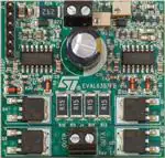
EVAL6393FB
Low voltage full-bridge demonstration board based on the L6393
advanced high voltage gate driver
Data brief
Features
■
~150 W drive capability (50 V - 3.0 Ar.m.s.)
■
Very low area occupation, all devices and
power switches in SMD package (no heatsink)
■
Fast-decay or slow-decay on-board constant
off-time peak current control
■
PWM voltage mode control with overcurrent
protection possible via external logic signals
■
Driver supply voltage on-board generation
directly from BUS voltage
■
Carefully optimized layout
EVAL6393FB
Description
The EVAL6393FB demonstrates how to use two
L6393 drivers to drive a single-phase load
through a full-bridge topology. This allows both
the direction and the value of the current flowing
into the load to be controlled. Typical loads, which
can be effectively driven by using this topology,
are single-phase BLDC motors, fans and HID
lamps. Thanks to the integrated features of the
L6393, the board has a very small footprint and
an optimized layout, and can be simply run by
applying the BUS voltage and a direction signal.
October 2012
Doc ID 023821 Rev 1
For further information contact your local STMicroelectronics sales office.
1/9
www.st.com
9
�Board description
1
EVAL6393FB
Board description
Table 1.
EVAL6393FB electrical specifications
Parameter
Value
Supply voltage range (VS)(1) (2)
32 V to 52 VDC
RMS output current rating (OUT x)
Up to 3.0 A
Driver supply voltage (VCC)
(3)
10 to 20 V
Logic control signals
0 to + 15 V
Operating temperature range
-40 to +125 °C
1. Minimum VS voltage restriction is due to biasing current of the Zener diode used to generate Vcc. This limit
can be decreased by changing R29 value or by opening JP3 and providing an externally generated Vcc
through connector J1.
2. Maximum VS voltage limit can be increased up to 580 V by replacing the power switches and bulk
capacitor C15 with components with adequate voltage ratings. Resistor R29 should be removed and an
externally generated Vcc should be provided through connector J1.
3. When externally supplied through J1 with JP3 opened, otherwise Vcc = 12 V.
Figure 1.
Jumper and connector location
On-board Vcc
generation jumper
BUS voltage
connector
Peak current
setting trimmer
Off-time setting
trimmer
Control signals and
optional external Vcc
connector
Slow/Fast Decay
selection jumpers
Load connector
AM12618v1
2/9
Doc ID 023821 Rev 1
�EVAL6393FB
Board description
Table 2.
Jumper and connector description
Name
Type
J1
Control signal connector
J2
Power output
Load connector
J3
Power supply
BUS power supply connector
JP1
Configuration jumper
To pull-up SD and/or BRAKE signal to VCC /3
JP2
Configuration jumper
To pull-up SD and/or BRAKE signal to CPOUT
JP3
Configuration jumper
To connect the on-board generated VCC to the supply pins
of the drivers
Table 3.
Function
Optional control signal and external VCC connector
Control signal connector pinout (J1)
Pin
Type
1
Power supply
Driver power supply VCC, open JP3 to provide externally
generated VCC
2
Power supply
GND
3
Digital input
Driver SD signal
4
Digital input
Driver BRAKE signal
5
Analog PWM input
6
Digital input
Table 4.
Description
Vctrl signal; used to change current limit threshold
DIR signal; sets current direction
Current peak detection settings
Pin
Type
Description
TR1
Variable resistor
Used to adjust constant off-time duration after overcurrent
detection
TR2
Variable resistor
Used to adjust overcurrent detection threshold Ipk
Ipk = V(CP-)/[R10//R11//R12//R13]
Table 5.
Control scheme configuration
Description
Jumper configuration
Constant off-time peak current control with slowdecay
JP1 closed on !SD and JP2 closed on !BRAKE
Constant off-time peak current control with fastdecay
JP1 closed on !SD and JP2 closed on !SD
PWM voltage control with slow-decay overcurrent JP1 open, JP2 closed on !BRAKE and !SD
protection
externally provided through J1
PWM voltage control with fast-decay overcurrent
protection
JP1 open, JP2 closed on !SD and !BRAKE
externally provided through J1
Doc ID 023821 Rev 1
3/9
�JP1
Vcc
4/9
Doc ID 023821 Rev 1
Vs
R18
7.5k
R6
24k
R22
47k
Q3
1
C7
4.7uF
DZ2
12V
SOD123
R29
2K4
1W
Vcc
C17
100nF
JP2
J1
2
3
P12V
C13
100nF
2N7002
JP3
!BRAKE
MMSZ4683
SOD123
DZ1
!SD
DIR
Vcc
1k
C11
33pF
C14
10uF
R14
Vcc
Vcc
R26
7.5k
Vcc
R20
24k
C16
33pF
C9
1uF
C2
1uF
Vs
R3
47k
R24
47k
Vs
1
2
DT
Vcc
J3
7
U2
GND
8
9
10
12
13
14
R27
3.9k
R25
24k
8
9
10
12
13
14
TR2
500
R8
10k
R5
30k
Vcc
CP+
+
- CP-
LVG
OUT
HVG
Boot
Vcc
CP+
+
- CP-
LVG
OUT
HVG
Boot
C6
4.7uF
Vctrl
BRAKE
SD
Phase
L6393
U1
GND
6 CPOut
5
4
3
2
!SD
7
1
!BRAKE
DT
Vcc
BRAKE
SD
Phase
6 CPOut
5
!DIR
C5
5.6nF
TR1
200k
R4
30k
C15
100uF
63V
C10
100nF
Vcc
C3
100nF
3
!BRAKE
4
2
1
!SD
L6393
1K
R30
C12
22nF
C18
33pF
C8
470nF
C1
470nF
DIR
C4
1nF
1k
R9
D4
D3
D2
D1
LL4148
51
R23
51
R21
LL4148
LL4148
51
R2
51
R1
LL4148
STD35NF06
1
Q5
STD35NF06
1
Q4
STD35NF06
1
Q2
STD35NF06
STD35N
1
Q1
3
2
3
2
Vs
3
2
3
2
Vs
R10
0R15
1W 1%
R11
0R15
1W 1%
R12
0R15
1W 1%
R13
0R15
1W 1%
OUTB
OUTA
2
1
J2
Figure 2.
Vcc
!SD
!BRAKE
Vctrl
DIR
1
2
3
4
5
6
Board description
EVAL6393FB
EVAL6393FB schematic
AM12619v1
�EVAL6393FB
Board description
Table 6.
EVAL6393FB bill of material
Reference
Value
C1, C8
470 nF, 25 V
SMT ceramic capacitor, 0805
C2, C9
1 µF, 25 V
SMT ceramic capacitor, 0805
C3, C10, C13, C17
100 nF, 25 V
SMT ceramic capacitor, 0603
C4
1 nF, 25 V
SMT ceramic capacitor, 0603
C5
5.6 nF, 25 V
SMT ceramic capacitor, 0603
C6, C7
4.7 µF
SMT ceramic capacitor, 0805
C11, C16, C18
33 pF, 25 V
SMT ceramic capacitor, 0603
C12
22 nF, 25 V
SMT ceramic capacitor, 0805
C14
10 µF, 25 V
SMT ceramic capacitor, 1206
C15
100 µF, 63 V
Radial lead electrolytic capacitor (D 10 mm, H 12.5 mm)
D1, D2, D3, D4
LL4148
DZ1
MMSZ4683
DZ2
Description
Fast switching diode, SOD80
3 V Zener diode, SOD123
12 V Zener diode, SOD123
J1
1x6 strip, 2.54 mm pitch
J2, J3
1x2 screw PCB terminal block, 5.08 mm pitch
JP1, JP2
2- way solder jumper
JP3
Solder jumper
Q1, Q2, Q4, Q5
STD35NF06
Q3
2N7002
R1, R2, R21, R23
51 Ω
SMT resistor, 0603
R3, R22, R24
47 kΩ
SMT resistor, 0603
R4, R5
30 kΩ
SMT resistor, 0603
R6, R20, R25
24 kΩ
SMT resistor, 0603
R8
10 kΩ
SMT resistor, 0603
R9, R14, R30
1 kΩ
SMT resistor, 0603
R10, R11, R12, R13
60 V, 35 A N-channel power MOSFET in DPAK
60 V, 0.2 A N-channel power MOSFET in SOT23
1% 1 W SMT resistor, 2512
R18, R26
7.5 kΩ
SMT resistor, 0603
R27
3.9 kΩ
SMT resistor, 0603
R29
Ω
TR1
200 kΩ
SMT trimmer
TR2
500 Ω
SMT trimmer
U1, U2
L6393D
5% 1W SMT resistor, 2512
Half-bridge gate driver, in SO14
Doc ID 023821 Rev 1
5/9
�Board description
Figure 3.
EVAL6393FB
EVAL6393FB – layout (top layer)
AM12620v1
Figure 4.
EVAL6393FB – layout (bottom layer)
AM12621v1
6/9
Doc ID 023821 Rev 1
�EVAL6393FB
Figure 5.
Board description
EVAL6393FB – layout (component placement view)
AM12622v1
Doc ID 023821 Rev 1
7/9
�Revision history
2
EVAL6393FB
Revision history
Table 7.
8/9
Document revision history
Date
Revision
23-Oct-2012
1
Changes
Initial release.
Doc ID 023821 Rev 1
�EVAL6393FB
Please Read Carefully:
Information in this document is provided solely in connection with ST products. STMicroelectronics NV and its subsidiaries (“ST”) reserve the
right to make changes, corrections, modifications or improvements, to this document, and the products and services described herein at any
time, without notice.
All ST products are sold pursuant to ST’s terms and conditions of sale.
Purchasers are solely responsible for the choice, selection and use of the ST products and services described herein, and ST assumes no
liability whatsoever relating to the choice, selection or use of the ST products and services described herein.
No license, express or implied, by estoppel or otherwise, to any intellectual property rights is granted under this document. If any part of this
document refers to any third party products or services it shall not be deemed a license grant by ST for the use of such third party products
or services, or any intellectual property contained therein or considered as a warranty covering the use in any manner whatsoever of such
third party products or services or any intellectual property contained therein.
UNLESS OTHERWISE SET FORTH IN ST’S TERMS AND CONDITIONS OF SALE ST DISCLAIMS ANY EXPRESS OR IMPLIED
WARRANTY WITH RESPECT TO THE USE AND/OR SALE OF ST PRODUCTS INCLUDING WITHOUT LIMITATION IMPLIED
WARRANTIES OF MERCHANTABILITY, FITNESS FOR A PARTICULAR PURPOSE (AND THEIR EQUIVALENTS UNDER THE LAWS
OF ANY JURISDICTION), OR INFRINGEMENT OF ANY PATENT, COPYRIGHT OR OTHER INTELLECTUAL PROPERTY RIGHT.
UNLESS EXPRESSLY APPROVED IN WRITING BY TWO AUTHORIZED ST REPRESENTATIVES, ST PRODUCTS ARE NOT
RECOMMENDED, AUTHORIZED OR WARRANTED FOR USE IN MILITARY, AIR CRAFT, SPACE, LIFE SAVING, OR LIFE SUSTAINING
APPLICATIONS, NOR IN PRODUCTS OR SYSTEMS WHERE FAILURE OR MALFUNCTION MAY RESULT IN PERSONAL INJURY,
DEATH, OR SEVERE PROPERTY OR ENVIRONMENTAL DAMAGE. ST PRODUCTS WHICH ARE NOT SPECIFIED AS "AUTOMOTIVE
GRADE" MAY ONLY BE USED IN AUTOMOTIVE APPLICATIONS AT USER’S OWN RISK.
Resale of ST products with provisions different from the statements and/or technical features set forth in this document shall immediately void
any warranty granted by ST for the ST product or service described herein and shall not create or extend in any manner whatsoever, any
liability of ST.
ST and the ST logo are trademarks or registered trademarks of ST in various countries.
Information in this document supersedes and replaces all information previously supplied.
The ST logo is a registered trademark of STMicroelectronics. All other names are the property of their respective owners.
© 2012 STMicroelectronics - All rights reserved
STMicroelectronics group of companies
Australia - Belgium - Brazil - Canada - China - Czech Republic - Finland - France - Germany - Hong Kong - India - Israel - Italy - Japan Malaysia - Malta - Morocco - Philippines - Singapore - Spain - Sweden - Switzerland - United Kingdom - United States of America
www.st.com
Doc ID 023821 Rev 1
9/9
�