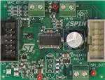
EVAL6470
Fully integrated microstepping motor driver using the L6470
Data brief
Features
■
Voltage range from 8 V to 45 V
■
Phase current up to 3 Ar.m.s.
■
SPI with daisy-chain feature
■
Socket for external resonator or crystal
■
SW input
■
Thermal resistance junction-to-ambient of 40
°C/W (typical)
■
Suitable to be used in combination with
STEVAL-PCC009V2
Description
The EVAL6470 demonstration board is a fully
integrated microstepping motor driver. In
combination with the STEVAL-PCC009V2
communication board and the dSPIN Evaluation
Software, the board allows the engineer to
investigate all the features of the L6470 device.
)
(s
)
s
(
ct
u
d
o
r
P
e
t
e
l
o
s
b
O
t
c
u
d
o
r
In particular, the board can be used to check the
voltage mode driving and to regulate the L6470
parameters in order to fit the application
requirements.
P
e
t
e
l
o
Two or more EVAL6470 can be driven by a single
communication board making the demonstration
board suitable for the evaluation of L6470 in multimotor applications.
s
b
O
March 2011
Doc ID 018622 Rev 1
For further information contact your local STMicroelectronics sales office.
1/11
www.st.com
11
�Board description
EVAL6470
1
Board description
Figure 1.
EVAL6470 demonstration board jumper and connector locations
)
s
(
ct
u
d
o
r
P
e
t
e
l
o
)
(s
s
b
O
t
c
u
d
o
r
P
e
t
e
l
o
s
b
O
2/11
Doc ID 018622 Rev 1
�EVAL6470
Board description
Table 1.
EVAL6470: jumper and connector description
Name
Type
J4
Power supply
Board power supply
J2
Power outputs
Bridge A outputs
J3
Power outputs
Bridge B outputs
J10
SPI connector
Master SPI connector
J11
SPI connector
Slave SPI connector
SW
NM test point
External switch connector
VS
Test point
Motor supply voltage
VREG
Test point
Internal 3 V regulator output
VDD
Test point
Logic interface voltage
GND
Test point
Ground
JP7
Jumper
Selects SPI connector PWM2 GPIO functionality
JP2
Jumper
Daisy chain termination
JP5
Jumper
EXT_VDD (SPI connector) to VDD connection
JP3
Jumper
VDD to VREG connection
JP4
Jumper
Table 2.
t
e
l
o
bs
Selects ADCIN source
O
)
od
Pr
3
4
Description
L6470 BUSY open drain output
2
O
u
d
o
r
P
e
t(s
uc
1
o
s
b
)
s
(
ct
EVAL6470: master SPI connector pinout (J10)
Pin number
e
t
e
l
Function
L6470 FLAG open drain output
Ground
EXT_VDD (can be used as external logic power supply)
5
SPI master in, slave out signal (connected to L6470 SDO output through
daisy chain termination jumper JP2)
6
SPI serial clock signal (connected to L6470 CK input)
7
SPI master out, slave in signal (connected to L6470 SDI input)
8
SPI slave select signal (connected to L6470 CS input)
9
PWM1 input
10
PWM2 input
Doc ID 018622 Rev 1
3/11
�Board description
EVAL6470
Table 3.
EVAL6470: slave SPI connector pinout (J11)
Pin number
Table 4.
Description
1
L6470 BUSY open drain output
2
L6470 FLAG open drain output
3
Ground
4
EXT_VDD (can be used as external logic power supply)
5
SPI master in, slave out signal (connected to pin 5 of J10)
6
SPI serial clock signal (connected to L6470 CK input)
7
SPI master out, slave in signal (connected to L6470 SDO output)
8
SPI slave select signal (connected to L6470 CS input)
9
PWM1 input
10
PWM2 input
u
d
o
r
P
e
EVAL6470: electrical specification (recommended values)
let
Parameter
Supply voltage range (VS)
8 to 45 V
o
s
b
Output current rating
O
)
Logic interface voltage (VDD)
t(s
Logic inputs voltage range
uc
Operating temperature range
od
L6470H thermal resistance junction-to-ambient
r
P
e
Value
Up to 3 Arms
Logic supply voltage (VREG)
3.3 V (when externally supplied)
3.3 V or 5 V (when externally supplied)
0 to +5 V
–25 to +125 °C
40 °C/W
t
e
l
o
s
b
O
4/11
)
s
(
ct
Doc ID 018622 Rev 1
�#��
���P&
#�
���P&
Doc ID 018622 Rev 1
�
07-�
N#3
#+
3$)
3$/
37
34#+ ,����
�
�
/3#).
/3#/54
5�
6$$
�
�
��
�
��
��
!$#).
37
34#+
34"9
&,!'
"539
��
��
��
��
�
��
34#+
�34"9
�&,!'
�"539
!$#).
37
/3#/54
/3#).
�� ��
2��
0'.$
0'.$
� �� ��
!'.$
/54�"
/54�"
/54�!
/54�!
#0 63!
63"
63!
63"
�� � ��
,����
u
d
o
��
�#3
#+
3$)
3$/
$'.$
�
"AT��37
34 �
#�
��N&
���6
$�
#�
���N&���6
6$$
6"//4
62%'
�� �
62%'
r
P
e
":8���#�6�
.#3
#+
3$)
3$/
34"9 &,!' "539
$�
07-�
s
b
O
t
e
l
o
#��
�N&
�
2�
d
o
r
t
c
u
2�
���N&
#��
*0�
�
)
(s
2�
6$$
�
s
b
O
2�
�
P
e
t
e
l
o
2�
2�
����6
����6
��
��
��
�
63
�
40�
'.$
�
�
�
�
!-�����
*�
#/.�
#/.�
*�
Figure 2.
2�
63
EVAL6470
Board description
EVAL6470 schematic - part 1
)
s
(
ct
5/11
�6/11
Doc ID 018622 Rev 1
#�
���N&
#�
.-
.-
9�
#�
.-
/3#/54
�
�
#�
���N&
40�
6$$
�
#��
��&����6
�
/3#/54
#��
��&����6
� .-
9�
62%'
/3#) .
#�
���N&
40�
62%'
�
6$$
3$/
-)3/
3$)
07-�
"539
t
e
l
o
s
b
O
/3#).
9�AND9�FOOTPRINTSAREPOSITIONED
SOASTOAXTAL�9� ORARESONATOR�9� CAN
BEINDIFFERENTLYMOUNTED�
#� �
���&��6
�
40�
63
3$/
62%'
)
(s
#/.�
�
�
�
�
*0�
t
e
l
o
P
e
d
o
r
63
�
4ERMINATION
*0�
�
6$$
s
b
O
t
c
u
*�
�
*0�
34"9
�
�
�
�
�
��
�
�
�
�
��
�
07-�
#/.��P
*��
#/.��P
*��
*0�
�
�
�
�
�
�
�
�
�
�
�
#+
N#3
07-�
&,!'
#+
N#3
07-�
&,!'
34#+
r
P
e
u
d
o
*�
�
%XTERNALSWITCH
CONNECTOR
)
s
(
ct
37
2�
#��
��N&
37
37
!-�����
%84?6$$
#+
N#3
07-�
&,!'
%84?6$$
'0)/)NPUTFUNCTIONSELECTION
!44%.4)/.�!LLTHEJUMPERSINTHECHAIN
MUSTBESETWITHTHESAMEFUNCTION�
-)3/
3$/
07-�
"539
-)3/
3$)
07-�
"539
Figure 3.
-)3/
%84?6$$
Board description
EVAL6470
EVAL6470 schematic - part 2
�EVAL6470
Board description
Table 5.
EVAL6470: component list
Part reference
Part value
Part description
C1
100 nF
50 V ceramic capacitor
C2
10 nF
63 V ceramic capacitor
C3, C8
100 nF
Ceramic capacitor
C4
100 µF
63 V electrolytic capacitor
C5
220 nF
16 V ceramic capacitor
C6, C7
NM
Ceramic capacitor
C9, C10
100 pF
Ceramic capacitor
C11
1 nF
Ceramic capacitor
C12
3.3 nF
Ceramic capacitor
C13
10 nF
C14
10 µF
C15
47 µF
D1
BAT46SW
D2
BZX284C3V6
JP5
O
)
JP4
t(s
JP7
c
u
d
J5
e
t
e
l
O
o
s
b
u
d
o
Ceramic capacitor
6.3 V ceramic capacitor
r
P
e
6.3 V ceramic capacitor
let
o
s
b
JP2, JP3
J2, J3, J4
)
s
(
ct
Low drop diode couple
3.6 V Zener diode
Jumper 2 x 1
Jumper 2 x 1
Jumper 3 x 1
Jumper 3 x 1
Connector
NM
Strip pin
o
r
P
R1
31.6 kΩ
Resistor 1%
R2
8.2 kΩ
Resistor 1%
R5, R6, R7
39 kΩ
Resistor 1%
R9
10 kΩ
Resistor 1%
R3
200 kΩ
Trimmer
R8
100 Ω
Resistor 1%
R10
0Ω
Resistor 1/8 W
J10
Vertical 5 x 2 male connector
J11
Vertical 5 x 2 male connector
TP5
Test point
TP4, TP6
Test point
U1
L6470H
L6470 dSPIN
Y1
NM
Crystal
Y2
NM
Ceramic resonator
Doc ID 018622 Rev 1
7/11
�Board description
Figure 4.
EVAL6470
EVAL6470 layout (top layer)
)
s
(
ct
u
d
o
r
P
e
Figure 5.
s
b
O
EVAL6470 layout (bottom layer)
)
(s
t
e
l
o
t
c
u
d
o
r
P
e
t
e
l
o
s
b
O
8/11
Doc ID 018622 Rev 1
�EVAL6470
2
Connection to IBU universal interface board
Connection to IBU universal interface board
The EVAL6470 should be connected to the interface board (STEVAL-PCC009V2 or
STEVAL-PCC009V1), and the following steps performed:
2.1
1.
Connect the interface board to the PC through the USB cable
2.
If requested, install interface board drivers
3.
Verify interface board operation (check if operation LED diode is turned on)
4.
Connect the interface board 10-pin connector to the EVAL6470 J10 connector (SPI_IN)
through the 10-pole flat cable
5.
Connect motor phases to the EVAL6470 J2 and J3 connectors
6.
Connect the power supply (8 V to 45 V) to the EVAL6470 J4 connector
7.
Start the dSPIN Evaluation tool.
)
s
(
ct
u
d
o
Daisy-chain mode
r
P
e
More EVAL6470 boards can be connected in daisy chain mode. This way you can control up
to eight motors using a single communication board (STEVAL-PCC009V2 only).
t
e
l
o
To drive two or more boards in daisy chain configuration:
Connect the interface board to the PC through the USB cable
2.
If requested, install the interface board drivers
3.
Verify interface board operation (check if the operation LED diode is turned on)
4.
Connect the interface board 10-pin connector to the first EVAL6470 J10 connector
(SPI_IN) through the 10-pole flat cable
)
(s
t
c
u
5.
Open the JP2 jumper of EVAL6470
6.
Connect the J11 connector (SPI_OUT) of the previous EVAL6470 to the J10 connector
(SPI_IN) of the next one through the 10-pole flat cable
7.
Repeat point 5 and 6 for all the others board of the chain but the last one.
8.
9.
s
b
O
d
o
r
P
e
t
e
l
o
Caution:
s
b
O
1.
Check the JP2 jumpers of EVAL6470 boards: all the jumpers but the last one should be
opened
Check the JP7 jumpers of EVAL6470 boards: all the jumpers should be in the same
configuration (STCK or STBY)
Increasing the number of devices connected in chain could degrade SPI communication
performances. If communication issues are founded, try to reduce SPI clock speed.
Figure 6.
Daisy chain configuration
5FSNJOBUJPO�
KVNQFS�DMPTFE
5FSNJOBUJPO�
KVNQFS�PQFO
*OUFSGBDF
CPBSE
45&7"-�1$$���7�
+��
+1�
+��
&7"-����
�TU�CPBSE
Doc ID 018622 Rev 1
+��
+1�
+��
&7"-����
-BTU�CPBSE
9/11
�Revision history
3
EVAL6470
Revision history
Table 6.
Document revision history
Date
Revision
22-Mar-2010
1
Changes
Initial release.
)
s
(
ct
u
d
o
r
P
e
t
e
l
o
)
(s
s
b
O
t
c
u
d
o
r
P
e
t
e
l
o
s
b
O
10/11
Doc ID 018622 Rev 1
�EVAL6470
)
s
(
ct
Please Read Carefully:
u
d
o
Information in this document is provided solely in connection with ST products. STMicroelectronics NV and its subsidiaries (“ST”) reserve the
right to make changes, corrections, modifications or improvements, to this document, and the products and services described herein at any
time, without notice.
r
P
e
All ST products are sold pursuant to ST’s terms and conditions of sale.
Purchasers are solely responsible for the choice, selection and use of the ST products and services described herein, and ST assumes no
liability whatsoever relating to the choice, selection or use of the ST products and services described herein.
t
e
l
o
No license, express or implied, by estoppel or otherwise, to any intellectual property rights is granted under this document. If any part of this
document refers to any third party products or services it shall not be deemed a license grant by ST for the use of such third party products
or services, or any intellectual property contained therein or considered as a warranty covering the use in any manner whatsoever of such
third party products or services or any intellectual property contained therein.
)
(s
s
b
O
UNLESS OTHERWISE SET FORTH IN ST’S TERMS AND CONDITIONS OF SALE ST DISCLAIMS ANY EXPRESS OR IMPLIED
WARRANTY WITH RESPECT TO THE USE AND/OR SALE OF ST PRODUCTS INCLUDING WITHOUT LIMITATION IMPLIED
WARRANTIES OF MERCHANTABILITY, FITNESS FOR A PARTICULAR PURPOSE (AND THEIR EQUIVALENTS UNDER THE LAWS
OF ANY JURISDICTION), OR INFRINGEMENT OF ANY PATENT, COPYRIGHT OR OTHER INTELLECTUAL PROPERTY RIGHT.
t
c
u
UNLESS EXPRESSLY APPROVED IN WRITING BY AN AUTHORIZED ST REPRESENTATIVE, ST PRODUCTS ARE NOT
RECOMMENDED, AUTHORIZED OR WARRANTED FOR USE IN MILITARY, AIR CRAFT, SPACE, LIFE SAVING, OR LIFE SUSTAINING
APPLICATIONS, NOR IN PRODUCTS OR SYSTEMS WHERE FAILURE OR MALFUNCTION MAY RESULT IN PERSONAL INJURY,
DEATH, OR SEVERE PROPERTY OR ENVIRONMENTAL DAMAGE. ST PRODUCTS WHICH ARE NOT SPECIFIED AS "AUTOMOTIVE
GRADE" MAY ONLY BE USED IN AUTOMOTIVE APPLICATIONS AT USER’S OWN RISK.
d
o
r
P
e
t
e
l
o
Resale of ST products with provisions different from the statements and/or technical features set forth in this document shall immediately void
any warranty granted by ST for the ST product or service described herein and shall not create or extend in any manner whatsoever, any
liability of ST.
s
b
O
ST and the ST logo are trademarks or registered trademarks of ST in various countries.
Information in this document supersedes and replaces all information previously supplied.
The ST logo is a registered trademark of STMicroelectronics. All other names are the property of their respective owners.
© 2011 STMicroelectronics - All rights reserved
STMicroelectronics group of companies
Australia - Belgium - Brazil - Canada - China - Czech Republic - Finland - France - Germany - Hong Kong - India - Israel - Italy - Japan Malaysia - Malta - Morocco - Philippines - Singapore - Spain - Sweden - Switzerland - United Kingdom - United States of America
www.st.com
Doc ID 018622 Rev 1
11/11
�


 工商网监
湘ICP备2023018690号
工商网监
湘ICP备2023018690号
