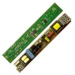
EVAL6520-1421
14 W / 21 W T5 miniature ballast driven by L6520
and STT13005D bipolar transistors
Data brief
Features
■
Drives either T5-14W-HE or T5-21W-HE lamps
■
Standard form factor (19 mm x 120 mm)
■
Compliance with IEC61347-2-3, IEC61000-2-3
and EN55022 Class-C
Description
The EVAL6520-1421 is a demonstration board
able to drive either a 14 W or 21 W linear T5
fluorescent lamp with the L6520 low voltage
ballast controller.
EVAL6520-1421
The half bridge consists of NPN high voltage
power transistors driven by a suitable pulse
transformer.
November 2011
Doc ID 018537 Rev 2
For further information contact your local STMicroelectronics sales office.
1/16
www.st.com
16
�Contents
EVAL6520-1421
Contents
1
Introduction . . . . . . . . . . . . . . . . . . . . . . . . . . . . . . . . . . . . . . . . . . . . . . . . 3
2
Board description . . . . . . . . . . . . . . . . . . . . . . . . . . . . . . . . . . . . . . . . . . . 4
3
Board performance . . . . . . . . . . . . . . . . . . . . . . . . . . . . . . . . . . . . . . . . . . 7
4
Application specifications . . . . . . . . . . . . . . . . . . . . . . . . . . . . . . . . . . . . 9
5
Bill of material and board schematics . . . . . . . . . . . . . . . . . . . . . . . . . . 10
5.1
Board schematic . . . . . . . . . . . . . . . . . . . . . . . . . . . . . . . . . . . . . . . . . . . . 12
Appendix A Magnetic components data. . . . . . . . . . . . . . . . . . . . . . . . . . . . . . . . 13
Revision history . . . . . . . . . . . . . . . . . . . . . . . . . . . . . . . . . . . . . . . . . . . . . . . . . . . . 15
2/16
Doc ID 018537 Rev 2
�EVAL6520-1421
1
Introduction
Introduction
The L6520 low voltage ballast controller is intended to drive extremely compact applications
based on either MOSFETs or bipolar transistors.
The EVAL6520-1421 is capable of driving either a T5-14W-HE or T5-21W-HE lamp, with the
same miniatured (16 mm wide) ballast.
The selection of both the resonant components and the bipolar transistors, together with the
design of the suitable pulse transformer, and IC power supply is also described.
Doc ID 018537 Rev 2
3/16
�Board description
2
EVAL6520-1421
Board description
The board is supplied by any AC voltage in the European mains range and does not need
any power factor correction having an input power of less than 25 W.
The half bridge voltage is obtained by filtering the rectified input voltage. This allows the use
of a cheaper bulk capacitor and bipolar transistors.
The selection of a target condition is required by the range of the input voltage together with
the necessity to drive two different kinds of lamps. In particular, the best driving condition
and the best efficiency is obtained at 240 Vac with a 14 W lamp connected.
An EMI filter is placed at the board’s input to meet IEC61000 standards.
The lamp's cathodes are current preheated to make the ballast choke more compact thanks
to the absence of auxiliary windings.
The resonant network design starts from the selection of the resonant capacitor (C10) that
corresponds to the desired ballast efficiency. The inductance (L1) can be obtained by the
following equation:
Equation 1
1
Lamp
R
=
1
R
Lamp
+ j ωC
V HB
⋅
j ωL
RES
RES
1
+
1
Lamp
R
+ j ωC
RES
Lamp
VHB is the effective voltage obtained across the half bridge along one mains cycle. The
lower voltage is obtained at 50 Hz and can be approximately computed as:
Equation 2
VHB
⎛ 2
⎞
= ⎜⎜
⋅ VIN − VF ⎟⎟ +
⎝ 2
⎠
2
⎛ 2
⎞ 1.54 ⋅ 10 5 ⋅ P
LAMP
⎜
⎟
⋅
V
−
V
⎜ 2
IN
F⎟ −
fMAINS ⋅ COUT
⎝
⎠
where:
●
VF is the forward voltage drop of the rectifier bridge (1 V typ.)
●
VIN is the RMS value of the input voltage
●
COUT is the value of the bulk capacitor in µF (In this case C3 = 4.7 µF has been
selected)
A resonant capacitor equal to 3.9 nF has been selected and resonant inductor equal to 3
mH has been calculated.
4/16
Doc ID 018537 Rev 2
�EVAL6520-1421
Board description
It is now possible to estimate the ignition frequency, which must be higher than 46 kHz
(minimum programmable value), and the minimum preheating frequency that guarantees a
preheating voltage higher than 130 Vrms, as required by the lamp specifications.
Equation 3
VPH−IGN
VPFC ⋅ 2
1
⋅
π
jωCRES
=
1
+ jωLRES
jωCRES
A preheating frequency equal to 70 kHz has been selected by connecting a 2.49 kΩ resistor
(R5) between the FPRE pin and GND.
The half bridge is based on two STT13005D power bipolar transistors (Q1 and Q2). Both the
high side and low side transistor are driven by a pulse transformer (T2).
To design this pulse transformer, the following parameters must be taken into account:
●
Maximum available spacing on the PCB: this determines the core dimension.
●
Maximum magnetizing current (Imag,rms) on the primary side of the transformer: this
current causes core losses to not be transferred as a useful signal on the secondary
side of the transformer. To minimize it, a higher primary inductance should be adopted.
Typical inductances are between 6 mH and 40 mH, depending on the core dimension
and the core permeability.
●
Primary to secondary transfer ratio (n): the output voltage of a step-down transformer is
lower than the input voltage, whereas the output current is higher than the input
current. This helps to obtain higher DC currents with lower IC power dissipation. The
minimum Vbe(sat) must be guaranteed in any condition as well as the minimum IB that
guarantees the saturation condition of the BJT.
The Imag,rms(MAX) is selected lower than 10 mA when Vcc is equal to 13 V and a typical
storage time of 1.2 µs is considered, therefore the primary inductance must be:
Equation 4
1
− Tdt − Tsto − 200ns
Ton,max
2 ⋅ frun
9.42us - Tsto
Lpri ≥ Vcc ⋅
= 3 ⋅ Vcc
= 1.732 ⋅ Vcc
= 6.18mH
Imag,rms
Imag,rms
Imag,rms
3
The Vbe of the bipolar transistor can be calculated as follows (see Figure 2):
Equation 5
⎡
⎤
Ib
Vbe = Vpri ⋅ n − Ib ⋅ Rb = ⎢ Vcc − ⋅ (Rds, on_h + Rpri + Rds, on_l)⎥ ⋅ n − Ib ⋅ Rb
⎣
⎦
n
The Rds,on_h and the Rds,on_l are the ON resistances of the L6520 drivers and can be
considered equal to 10 Ω each.
Ib is equal to Ic/hfe, and can be considered equal to Ic/6. Ib times Rb can be set between
0.7 V and 1 V, during run mode: in this design Rb (R6 and R8) can be selected between 10
Ω and 13 Ω.
Doc ID 018537 Rev 2
5/16
�Board description
EVAL6520-1421
With these constraints the following is obtained:
Equation 6
⎡
⎤
0.46
Vbe = ⎢13 −
⋅ (20 + Rpri)⎥ ⋅ n − 0.76 = 13 ⋅ n - 9.2 - 0.46 ⋅ Rpri - 0.76 > 1.1 → 13 ⋅ n - 0.46 ⋅ Rpri > 11.6
⎣
⎦
n
Selecting an Rpri (R7) equal to 47 Ω, the minimum transfer ratio should be equal to 2.55.
n = 5.6 has been selected.
The PWM_det pin network is composed of 3x220 kΩ resistors (R11 to R13) together with a
47 pF speed-up capacitor (C11). The value of the speed-up capacitor also avoids a
misdetection of the hard switching.
During normal operation the IC absorbs the following currents from the Vcc:
1. Effective base currents of the BJTs divided by n (5.6). A 39 mA(MAX) is estimated.
2. Magnetizing current = 10 mA(MAX)
3. L6520 power consumption: 8 mA(MAX)
A maximum current of 57 mArms must be foreseen. For this reason, the IC power supply has
been connected in series with the resonant network (D4 and D5). This connection does not
interfere with the optimum preheating of the lamp’s cathodes, but introduces a little offset
(7.5 V typ.) into the lamp voltage.
This offset affects the EOL detection, but a different choice of values of the Zener diodes
(D6 and D7) makes the detection symmetrical. The two values, together with the resistance
values (R14 and R15), can be calculated through the following system of equations
(VLamp,MAX = 30 V and VLamp,min = -16 V):
Equation 7
⎧ VLamp,MAX = VEOL + VZ,D7 + IBIAS ⋅ (R14 + R15) + VF,D6
⎨
⎩ VLamp,min = VEOL − VZ,D6 − IBIAS ⋅ (R14 + R15) − VF,D7
Finally, a 4.7 µF is used as the Vcc bulk capacitor (C4) and two 100 nF ceramic capacitors
(C5) are placed close to the Vcc pins of the two ICs.
By allowing the startup network (R2 to R4) to pass through the upper cathode of the lamp,
the automatic re-lamp feature is easily obtained.
6/16
Doc ID 018537 Rev 2
�EVAL6520-1421
3
Board performance
Board performance
Figure 1.
EMI spectrum at nominal input voltage (230 Vac)
Figure 2.
Lamp voltage and current (T5 14 W HE)
Doc ID 018537 Rev 2
7/16
�Board performance
Figure 3.
8/16
EVAL6520-1421
Lamp voltage and current (T5 21 W HE)
Doc ID 018537 Rev 2
�EVAL6520-1421
4
Application specifications
Application specifications
Table 1 and 2 show the application specifications for the input and lamp requirements.
Table 1.
Table 2.
Input requirements
Parameter
Value
Unit
Input voltage
198 to 264
Vrms
Mains freq.
50 to 60
Hz
Input power
25
W max
Lamp requirements
Parameter
T5 - 14 W
Lamp current
Lamp voltage
T5 - 21 W
170 ± 30%
82 ± 6%
Unit
mArms
123 ± 6%
Vrms
Max. ignition voltage
1000
Vpk
Max. preheating voltage
130
Vrms
Doc ID 018537 Rev 2
9/16
�Bill of material and board schematics
5
Bill of material and board schematics
Table 3.
10/16
EVAL6520-1421
Bill of material
Reference
Value / part number
Rating
C1
100 nF
275 Vac
C2
100 nF
275 Vac
C3
4.7 µF
400 Vdc - 105 °C
C4
4.7 µF
50 Vdc
C5
100 nF
25 Vdc
C6
1 nF
25 Vdc
C7
100 nF
400 Vdc
C8
100 nF
25 Vdc
C9
1 nF
25 Vdc
C10
3.9 nF
1000 Vdc
C11
10 pF
500 Vdc
C12
100 nF
25 Vdc
C13
Not mounted
C14
22 nF
50 Vdc
R1
PCB fuse
6A-1s
R2
330 kΩ
R3
330 kΩ
R4
270 kΩ
R5
2.94 kΩ
R6
10 Ω
R7
47 Ω
R8
10 Ω
R9
470 Ω
R10
1.2 Ω
R11
220 kΩ
R12
220 kΩ
R13
220 kΩ
R14
560 kΩ
R15
560 kΩ
T1
2 x 33 mH CM-filter
Notes
Panasonic ECQ
P6392JU
0.1%
1%
440 mA / 250 Vac
Doc ID 018537 Rev 2
SCLE16333-ITACOIL
�EVAL6520-1421
Bill of material and board schematics
Table 3.
Bill of material (continued)
Reference
Value / part number
Rating
Notes
T2
5.6 : 1:1
12 mH
E0802-ITACOIL
(Figure 5)
L1
3 mH
0.9 A
E16113-ITACOIL
(Figure 6)
U1
L6520
Q1
STT13005D
Q2
STT13005D
D1
B6S-E3/80
D2
RB751V40T1
D3
RB751V40T1
D4
MMSD4148T1G
D5
BZT03C15
3W
D6
MM3Z6V8ST1
6.8 V Zener
D7
MM3Z6V8ST1
16 V Zener
J1
VIN connector
198-264 Vac
J2
Lamp connector
Doc ID 018537 Rev 2
11/16
�*�
2�
�
#�
Doc ID 018537 Rev 2
�
�
07-?DET
("#3
%/,
&02%
5�
#��
#��
$�
�5
�
�
�
�
2��
�
�
$�
�&
'.$
,3$
(3$
6##
�
�
�
�
#�
#�
#�
6CC
#�
2��
2��
�
2�
#�
2�
�
2��
2��
�
�
4�
�
�
�
�
�
$�
�
$�
2�
2�
$�
�
/54
#�
2��
(6
1�
1�
#��
#�
2�
�
,�
#��
�
2�
2�
�
$�
�
�
�
�
#��
*�
��7
��74�
$�
Figure 4.
���
���6AC
�
�
#�
4�
�
�
12/16
5.1
�
2�
Bill of material and board schematics
EVAL6520-1421
Board schematic
Board schematic
!-�����V�
�EVAL6520-1421
'
'
Pulse transformer (T2) datasheet
'
,
4
Figure 5.
Magnetic components data
#
Appendix A
Magnetic components data
AM07774v1
Doc ID 018537 Rev 2
13/16
�Magnetic components data
Figure 6.
EVAL6520-1421
Ballast choke (L1) datasheet
AM07475v1
14/16
Doc ID 018537 Rev 2
�EVAL6520-1421
Revision history
Revision history
Table 4.
Revision history
Date
Revision
Changes
07-Mar-2011
1
Initial release.
28-Nov-2011
2
Updated Section 2 and Table 3.
Doc ID 018537 Rev 2
15/16
�EVAL6520-1421
Please Read Carefully:
Information in this document is provided solely in connection with ST products. STMicroelectronics NV and its subsidiaries (“ST”) reserve the
right to make changes, corrections, modifications or improvements, to this document, and the products and services described herein at any
time, without notice.
All ST products are sold pursuant to ST’s terms and conditions of sale.
Purchasers are solely responsible for the choice, selection and use of the ST products and services described herein, and ST assumes no
liability whatsoever relating to the choice, selection or use of the ST products and services described herein.
No license, express or implied, by estoppel or otherwise, to any intellectual property rights is granted under this document. If any part of this
document refers to any third party products or services it shall not be deemed a license grant by ST for the use of such third party products
or services, or any intellectual property contained therein or considered as a warranty covering the use in any manner whatsoever of such
third party products or services or any intellectual property contained therein.
UNLESS OTHERWISE SET FORTH IN ST’S TERMS AND CONDITIONS OF SALE ST DISCLAIMS ANY EXPRESS OR IMPLIED
WARRANTY WITH RESPECT TO THE USE AND/OR SALE OF ST PRODUCTS INCLUDING WITHOUT LIMITATION IMPLIED
WARRANTIES OF MERCHANTABILITY, FITNESS FOR A PARTICULAR PURPOSE (AND THEIR EQUIVALENTS UNDER THE LAWS
OF ANY JURISDICTION), OR INFRINGEMENT OF ANY PATENT, COPYRIGHT OR OTHER INTELLECTUAL PROPERTY RIGHT.
UNLESS EXPRESSLY APPROVED IN WRITING BY TWO AUTHORIZED ST REPRESENTATIVES, ST PRODUCTS ARE NOT
RECOMMENDED, AUTHORIZED OR WARRANTED FOR USE IN MILITARY, AIR CRAFT, SPACE, LIFE SAVING, OR LIFE SUSTAINING
APPLICATIONS, NOR IN PRODUCTS OR SYSTEMS WHERE FAILURE OR MALFUNCTION MAY RESULT IN PERSONAL INJURY,
DEATH, OR SEVERE PROPERTY OR ENVIRONMENTAL DAMAGE. ST PRODUCTS WHICH ARE NOT SPECIFIED AS "AUTOMOTIVE
GRADE" MAY ONLY BE USED IN AUTOMOTIVE APPLICATIONS AT USER’S OWN RISK.
Resale of ST products with provisions different from the statements and/or technical features set forth in this document shall immediately void
any warranty granted by ST for the ST product or service described herein and shall not create or extend in any manner whatsoever, any
liability of ST.
ST and the ST logo are trademarks or registered trademarks of ST in various countries.
Information in this document supersedes and replaces all information previously supplied.
The ST logo is a registered trademark of STMicroelectronics. All other names are the property of their respective owners.
© 2011 STMicroelectronics - All rights reserved
STMicroelectronics group of companies
Australia - Belgium - Brazil - Canada - China - Czech Republic - Finland - France - Germany - Hong Kong - India - Israel - Italy - Japan Malaysia - Malta - Morocco - Philippines - Singapore - Spain - Sweden - Switzerland - United Kingdom - United States of America
www.st.com
16/16
Doc ID 018537 Rev 2
�


 工商网监
湘ICP备2023018690号
工商网监
湘ICP备2023018690号
