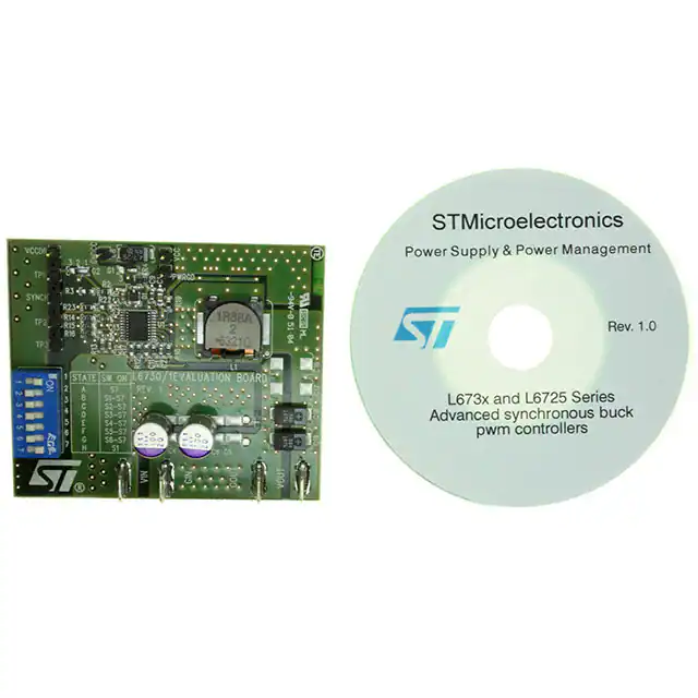
EVAL6730
L6730: 20A Demoboard
Data Brief
General description
L6730 demoboard realizes in a four layer PCB a step-down DC/DC converter and shows the
operation of the device in a general purpose application. The input voltage can range from
4.5 V to 14 V and the output voltage is at 3.3 V. The module can deliver an output current in
excess of 30A. The switching frequency is set at 400 KHz (controller free-running FSW) but it
can be increased up to 1 MHz. A 7 positions dip-switch allows to select the UVLO threshold
(5 V or 12 V Bus), the OVP intervention mode and the sink-mode current capability.
Demoboard picture
January 2007
Rev 1
For further information contact your local STMicroelectronics sales office.
1/9
www.st.com
�Features
1
EVAL6730
Features
Figure 1.
Demoboard schematic
VIN
3
2
1
D1
C3
C1
R2
SYNCH
VCCDR BOOT
GIN
R3
1
2
3
EAREF
9
U1
R4
C9
5
SGND
R22
TP2
C21
R23
TMASK
S/O/U
TP3
17
L6730
8
PGDelay
S1 R5
S2 R6
16
20
11
C10
R12
10
6
7
OCL
LGATE
R19
COMP
D2
PGND
PGOOD
GOUT
PWRGD
SS
R20
C15
OSC
VCCDR
R17
VFB
STATE
R16
C12R13
C13
R15
C14
SW ON
A
S7
B
S1-S7
C
S2-S7
S4 R8
D
S3-S7
S5 R9
E
S4-S7
S6R10
F
S5-S7
G
S6-S7
H
S1
R14
S7R11
2/9
C16-C19
C20
C11
S3 R7
Table 1.
VOUT
R21
Q4-6
4
3
1
L1
Q1-3
PHASE
13
19
C8
SYNCH
R18
HGATE
2
14
VCC
VCCDR
12
15
18
OCH
C7
G2
TP1
VCC
GNDCC
C2
R1
C4-C6
G1
Demoboard part list
Reference
Value
Manufacturer
Package
Supplier
R1
820 Ω
Neohm
SMD 0603
IFARCAD
R2
0Ω
Neohm
SMD 0603
IFARCAD
R3
N.C.
R4
10 Ω 1% 100 mW
Neohm
SMD 0603
IFARCAD
R5
11 KΩ 1% 100 mW
Neohm
SMD 0603
IFARCAD
R6
6.2 KΩ 1% 100 mW
Neohm
SMD 0603
IFARCAD
R7
4.3 KΩ 1% 100 mW
Neohm
SMD 0603
IFARCAD
R8
2.7 KΩ 1% 100 mW
Neohm
SMD 0603
IFARCAD
R9
1.8 KΩ 1% 100 mW
Neohm
SMD 0603
IFARCAD
R10
1.2 KΩ 1% 100 mW
Neohm
SMD 0603
IFARCAD
R11
2.7 KΩ 1% 100 mW
Neohm
SMD 0603
IFARCAD
R12
1 KΩ
Neohm
SMD 0603
IFARCAD
R13
2.7 KΩ 1% 100 mW
Neohm
SMD 0603
IFARCAD
�EVAL6730
Table 1.
Features
Demoboard part list (continued)
Reference
Value
Manufacturer
Package
Supplier
R14
1 KΩ 1% 100mW
Neohm
SMD 0603
IFARCAD
R15
1 KΩ 1% 100mW
Neohm
SMD 0603
IFARCAD
R16
4.7 KΩ 1% 100mW
Neohm
SMD 0603
IFARCAD
R17
N.C.
R18
2.2 Ω
Neohm
SMD 0603
IFARCAD
R19
2.2 Ω
Neohm
SMD 0603
IFARCAD
R20
10 KΩ 1% 100 mW
Neohm
SMD 0603
IFARCAD
R21
N.C.
R22
N.C.
R23
0Ω
Neohm
SMD 0603
IFARCAD
C1
220 nF
Kemet
SMD 0603
IFARCAD
C3-C7-C9-C15-C21
100 nF
Kemet
SMD 0603
IFARCAD
C2
1 nF.
Kemet
SMD 0603
IFARCAD
C4-C6
100 µF 20V
OSCON 20SA100M
RADIAL 10X10.5
SANYO
C8
4.7 µF 20V
AVX
SMA6032
IFARCAD
C10
10 nF
Kemet
SMD 0603
IFARCAD
C11
N.C.
C12
47 nF
Kemet
SMD 0603
IFARCAD
C13
1.5 nF
Kemet
SMD 0603
IFARCAD
C14
4.7nF
Kemet
SMD 0603
IFARCAD
C18-C19
330µF 6.3V
POSCAP 6TPB330M
SMD
SANYO
C20
N.C.
L1
1.8 µH
Panasonic
SMD
ST
D1
1N4148
ST
SOT23
IFARCAD
D2
STS1L30M
ST
DO216AA
ST
Q1-Q2
STS12NH3LL
ST
SO8
ST
Q4-Q5
STSJ100NH3LL
ST
SO8
ST
U1
L6730
ST
QFN 4x4 24L
ST
SWITCH
DIP SWITCH 7 POS.
Table 2.
ST
Other inductor manufacturer
Manufacturer
Series
Inductor value (µH)
Saturation current (A)
WURTH ELEKTRONIC
744318180
1.8
20
SUMIDA
CDEP134-2R7MC-H
2.7
15
EPCOS
HPI_13 T640
1.4
22
3/9
�Features
EVAL6730
Table 2.
Other inductor manufacturer
Manufacturer
Series
Inductor value (µH)
Saturation current (A)
TDK
SPM12550T-1R0M220
1
22
TOKO
FDA1254
2.2
14
HCF1305-1R0
1.15
22
HC5-1R0
1.3
27
Series
Capacitor value(µF)
Rated voltage (V)
C4532X5R1E156M
15
25
C3225X5R0J107M
100
6.3
NIPPON CHEMI-CON
25PS100MJ12
100
25
PANASONIC
ECJ4YB0J107M
100
6.3
COILTRONICS
Table 3.
Other capacitor manufacturer
Manufacturer
TDK
1.1
I/O description
Figure 2.
●
I/O description
Input (Vin-Gin):
The input voltage can range from 1.8 V to 14 V. If the input voltage is between 4.5 V and 14
V it can supply also the device (through the Vcc pin) and in this case the pin 1 and 2 of the
jumper G1 must be connected together.
●
Output (Vout-Gout):
The output voltage is fixed at 3.3 V but it can be changed by replacing the resistor R14 of the
output resistor divider:
R 16⎞
V O = V REF • ⎛ 1 + -------⎝
R ⎠
14
4/9
�EVAL6730
Features
The over-current-protection limit is set at 15 A but it can be changed by replacing the
resistors R1 and R12 (see OCL and OCH pin).
●
Vcc-Gndcc:
Using the input voltage to supply the controller no power is required at this input. However
the controller can be supplied separately from the power stage through the Vcc input (4.514V) and, in this case, jumper G1 must be left open.
●
VCCDR:
An internal LDO provides the power into the device. The input of this stage is the Vcc pin
and the output (5 V) is the VCCDR pin. The LDO can be bypassed, providing directly a 5 V
voltage from VCCDR and Gndcc. In this case the pins 1 and 3 of the jumper G1 must be
shorted.
●
TP1:
This pin can be used as an input or as a test point. If all the jumper G2 pins are shorted, TP1
can be used as a test point of the voltage at the EAREF pin.
If the pins 2 and 3 of G2 are connected together, TP1 can be used as an input to provide an
external reference for the internal error amplifier.
●
TP2:
This test point is connected to the Tmask pin.
●
TP3:
This test point is connected to the S/O/U pin.
●
SYNCH:
This pin is connected to the synch pin of the controller.
●
PWRGD:
This pin is connected to the PGOOD pin of the controller.
●
DIP SWITCH
Different positions of the dip switch correspond to different settings of the multifunction pin
(S/O/U) (CC/O/U).
Table 4.
Dip switch
UVLO
OVP
5V
Not latched
5V
SINK
Vsou/ VBCCDRB
DIP SWITCH
STATE
Not
0
S7
A
Not latched
Yes
0.2
S1-S7
B
5V
Latched
Not
0.3
S2-S7
C
5V
Latched
Yes
0.4
S3-S7
D
12 V
Not latched
Not
0.5
S4-S7
E
12 V
Not latched
Yes
0.6
S5-S7
F
12 V
Latched
Not
0.7
S6-S7
G
12 V
Latched
Yes
1
S1
H
CC
5/9
�Features
1.2
EVAL6730
Efficiency
The following figures show the demoboard efficiency versus load current for different values
of input voltage and switching frequency:
Figure 3.
Demoboard efficiency - Fsw=400 KHz
Fsw=400KHz
Vo=3.3V
EFFICIENCY
95.00%
90.00%
Vin=5V
85.00%
80.00%
Vin=12V
75.00%
1
3
5
7
9
11
13
15
Iout (A)
Figure 4.
Demoboard efficiency - Fsw=645 KHz
Fsw=645KHz
Vo=3.3V
EFFICIENCY
95.00%
90.00%
Vin=5V
85.00%
80.00%
Vin=12V
75.00%
70.00%
1
3
5
7
Iout (A)
6/9
9
11
13
15
�EVAL6730
Features
Figure 5.
Demoboard efficiency - Fsw=1 MHz
Fsw=1MHz
Vo=3.3V
95.00%
Vin=5V
EFFICIENCY
90.00%
85.00%
80.00%
Vin=12V
75.00%
70.00%
65.00%
60.00%
1
3
5
7
9
11
13
15
Iout (A)
Efficiency with 2xSTS12NH3LL+2XSTSJ100NH3LL
12V-->3.3V
EFFICIENCY (%)
Figure 6.
0.96
0.95
0.94
0.93
0.92
0.91
0.9
0.89
0.88
0.87
400KHz
700KHz
1MHz
3
5
7
9
11
13
15
17
19
OUTPUT CURRENT (A)
7/9
�Pictures of demoboard EVAL6730
EVAL6730
2
Pictures of demoboard EVAL6730
Figure 7.
PCB layout - top layer
Figure 8.
Figure 9.
PCB layout - Signal-ground layer
Figure 10. PCB layout - bottom layer
3
Revision history
Table 5.
8/9
PCB layout - power ground layer
Revision history
Date
Revision
03-Jan-2007
1
Changes
First issue
�EVAL6730
Please Read Carefully:
Information in this document is provided solely in connection with ST products. STMicroelectronics NV and its subsidiaries (“ST”) reserve the
right to make changes, corrections, modifications or improvements, to this document, and the products and services described herein at any
time, without notice.
All ST products are sold pursuant to ST’s terms and conditions of sale.
Purchasers are solely responsible for the choice, selection and use of the ST products and services described herein, and ST assumes no
liability whatsoever relating to the choice, selection or use of the ST products and services described herein.
No license, express or implied, by estoppel or otherwise, to any intellectual property rights is granted under this document. If any part of this
document refers to any third party products or services it shall not be deemed a license grant by ST for the use of such third party products
or services, or any intellectual property contained therein or considered as a warranty covering the use in any manner whatsoever of such
third party products or services or any intellectual property contained therein.
UNLESS OTHERWISE SET FORTH IN ST’S TERMS AND CONDITIONS OF SALE ST DISCLAIMS ANY EXPRESS OR IMPLIED
WARRANTY WITH RESPECT TO THE USE AND/OR SALE OF ST PRODUCTS INCLUDING WITHOUT LIMITATION IMPLIED
WARRANTIES OF MERCHANTABILITY, FITNESS FOR A PARTICULAR PURPOSE (AND THEIR EQUIVALENTS UNDER THE LAWS
OF ANY JURISDICTION), OR INFRINGEMENT OF ANY PATENT, COPYRIGHT OR OTHER INTELLECTUAL PROPERTY RIGHT.
UNLESS EXPRESSLY APPROVED IN WRITING BY AN AUTHORIZED ST REPRESENTATIVE, ST PRODUCTS ARE NOT
RECOMMENDED, AUTHORIZED OR WARRANTED FOR USE IN MILITARY, AIR CRAFT, SPACE, LIFE SAVING, OR LIFE SUSTAINING
APPLICATIONS, NOR IN PRODUCTS OR SYSTEMS WHERE FAILURE OR MALFUNCTION MAY RESULT IN PERSONAL INJURY,
DEATH, OR SEVERE PROPERTY OR ENVIRONMENTAL DAMAGE. ST PRODUCTS WHICH ARE NOT SPECIFIED AS "AUTOMOTIVE
GRADE" MAY ONLY BE USED IN AUTOMOTIVE APPLICATIONS AT USER’S OWN RISK.
Resale of ST products with provisions different from the statements and/or technical features set forth in this document shall immediately void
any warranty granted by ST for the ST product or service described herein and shall not create or extend in any manner whatsoever, any
liability of ST.
ST and the ST logo are trademarks or registered trademarks of ST in various countries.
Information in this document supersedes and replaces all information previously supplied.
The ST logo is a registered trademark of STMicroelectronics. All other names are the property of their respective owners.
© 2007 STMicroelectronics - All rights reserved
STMicroelectronics group of companies
Australia - Belgium - Brazil - Canada - China - Czech Republic - Finland - France - Germany - Hong Kong - India - Israel - Italy - Japan Malaysia - Malta - Morocco - Singapore - Spain - Sweden - Switzerland - United Kingdom - United States of America
www.st.com
9/9
�
很抱歉,暂时无法提供与“EVAL6730”相匹配的价格&库存,您可以联系我们找货
免费人工找货