AN2451
Application note
ST7540 FSK powerline transceiver
design guide for AMR
Introduction
The ST7540 reference design has been developed as a useful tool to demonstrate how a
small, high-performance powerline node can be built using the ST7540 FSK transceiver.
With this reference design, it is possible to evaluate the ST7540 features, in particular, its
transmitting and receiving performances through actual communication on the power line.
The ST7540 reference design may be considered to be composed of three main sections:
●
Power supply section, specifically tailored to match powerline coupling requirements
and to operate within a wide range of the input mains voltage
●
Modem and crystal oscillator section
●
Line coupling interface section
The coupling interface is designed to allow the ST7540 FSK transceiver to transmit and
receive on the mains using 72 kHz carrier frequencies, within the European CENELEC
standard A-band specified for automatic meter reading.
ST7540 reference design board with outline dimensions
52 mm
Figure 1.
76 mm
As it can be seen from the picture above, a special effort has been made to obtain a very
compact reference design board, while keeping the focus on transmission and receiving
performances.
Note:
January 2008
The information provided in this application note refers to EVALST7540-1 reference design
board.
Rev 2
1/55
www.st.com
�Contents
AN2451
Contents
1
Electrical characteristics . . . . . . . . . . . . . . . . . . . . . . . . . . . . . . . . . . . . . 7
2
Safety precautions . . . . . . . . . . . . . . . . . . . . . . . . . . . . . . . . . . . . . . . . . . 9
3
ST7540 FSK powerline transceiver description . . . . . . . . . . . . . . . . . . 10
4
Evaluation tools description . . . . . . . . . . . . . . . . . . . . . . . . . . . . . . . . . 11
5
Board description . . . . . . . . . . . . . . . . . . . . . . . . . . . . . . . . . . . . . . . . . . 13
5.1
5.2
Coupling interface . . . . . . . . . . . . . . . . . . . . . . . . . . . . . . . . . . . . . . . . . . 18
5.1.1
Tx active filter . . . . . . . . . . . . . . . . . . . . . . . . . . . . . . . . . . . . . . . . . . . . . 19
5.1.2
Tx passive filter . . . . . . . . . . . . . . . . . . . . . . . . . . . . . . . . . . . . . . . . . . . 20
5.1.3
Rx passive filter . . . . . . . . . . . . . . . . . . . . . . . . . . . . . . . . . . . . . . . . . . . 22
5.1.4
Input impedance . . . . . . . . . . . . . . . . . . . . . . . . . . . . . . . . . . . . . . . . . . 24
Conducted disturbances . . . . . . . . . . . . . . . . . . . . . . . . . . . . . . . . . . . . . . 25
5.2.1
Conducted emissions . . . . . . . . . . . . . . . . . . . . . . . . . . . . . . . . . . . . . . 25
5.2.2
Noise immunity . . . . . . . . . . . . . . . . . . . . . . . . . . . . . . . . . . . . . . . . . . . 26
5.3
Thermal design . . . . . . . . . . . . . . . . . . . . . . . . . . . . . . . . . . . . . . . . . . . . 29
5.4
Oscillator section . . . . . . . . . . . . . . . . . . . . . . . . . . . . . . . . . . . . . . . . . . . 32
5.5
Surge and burst protection . . . . . . . . . . . . . . . . . . . . . . . . . . . . . . . . . . . . 32
5.6
50-pin connector for the EVALCOMMBOARD . . . . . . . . . . . . . . . . . . . . . 35
5.7
Power supply . . . . . . . . . . . . . . . . . . . . . . . . . . . . . . . . . . . . . . . . . . . . . . 36
6
Performance and ping tests . . . . . . . . . . . . . . . . . . . . . . . . . . . . . . . . . . 41
7
Application ideas . . . . . . . . . . . . . . . . . . . . . . . . . . . . . . . . . . . . . . . . . . . 42
8
2/55
7.1
Three-phase architecture . . . . . . . . . . . . . . . . . . . . . . . . . . . . . . . . . . . . . 42
7.2
Zero crossing detector . . . . . . . . . . . . . . . . . . . . . . . . . . . . . . . . . . . . . . . 42
7.3
Received Signal Strength Indicator (RSSI) . . . . . . . . . . . . . . . . . . . . . . . 44
7.4
Nonisolated coupling . . . . . . . . . . . . . . . . . . . . . . . . . . . . . . . . . . . . . . . . 45
7.5
DC powerline applications . . . . . . . . . . . . . . . . . . . . . . . . . . . . . . . . . . . . 46
7.6
110 and 132.5 kHz coupling circuit . . . . . . . . . . . . . . . . . . . . . . . . . . . . . 46
Troubleshooting . . . . . . . . . . . . . . . . . . . . . . . . . . . . . . . . . . . . . . . . . . . 49
�AN2451
Contents
Appendix A Board layout . . . . . . . . . . . . . . . . . . . . . . . . . . . . . . . . . . . . . . . . . . . . 51
9
List of normative references . . . . . . . . . . . . . . . . . . . . . . . . . . . . . . . . . 54
10
Revision history . . . . . . . . . . . . . . . . . . . . . . . . . . . . . . . . . . . . . . . . . . . 54
3/55
�List of figures
AN2451
List of figures
Figure 1.
Figure 2.
Figure 3.
Figure 4.
Figure 5.
Figure 6.
Figure 7.
Figure 8.
Figure 9.
Figure 10.
Figure 11.
Figure 12.
Figure 13.
Figure 14.
Figure 15.
Figure 16.
Figure 17.
Figure 18.
Figure 19.
Figure 20.
Figure 21.
Figure 22.
Figure 23.
Figure 24.
Figure 25.
Figure 26.
Figure 27.
Figure 28.
Figure 29.
Figure 30.
Figure 31.
Figure 32.
Figure 33.
Figure 34.
Figure 35.
Figure 36.
Figure 37.
Figure 38.
Figure 39.
Figure 40.
Figure 41.
Figure 42.
Figure 43.
4/55
ST7540 reference design board with outline dimensions . . . . . . . . . . . . . . . . . . . . . . . . . . . 1
Typical curve for output current limit vs. RCL value . . . . . . . . . . . . . . . . . . . . . . . . . . . . . . . 9
ST7540 Transceiver block diagram . . . . . . . . . . . . . . . . . . . . . . . . . . . . . . . . . . . . . . . . . . 10
Complete evaluation system including a PC, an EVALCOMMBOARD and the
EVALST7540-1 board. . . . . . . . . . . . . . . . . . . . . . . . . . . . . . . . . . . . . . . . . . . . . . . . . . . . . 11
ST7540 powerline modem demonstration kit with control register window . . . . . . . . . . . . 12
Positioning of the various sections of the board . . . . . . . . . . . . . . . . . . . . . . . . . . . . . . . . . 13
Modem and coupling interface schematic . . . . . . . . . . . . . . . . . . . . . . . . . . . . . . . . . . . . . 14
Power supply schematic . . . . . . . . . . . . . . . . . . . . . . . . . . . . . . . . . . . . . . . . . . . . . . . . . . . 15
Schematic of Rx and Tx filters . . . . . . . . . . . . . . . . . . . . . . . . . . . . . . . . . . . . . . . . . . . . . . 19
Measured frequency response of the Tx active filter (typical curve). . . . . . . . . . . . . . . . . . 20
Simulated frequency response of the Tx active filter with components tolerance effect. . . 20
Measured frequency response of the Tx active + passive filters connected to the CISPR
network (typical curve) . . . . . . . . . . . . . . . . . . . . . . . . . . . . . . . . . . . . . . . . . . . . . . . . . . . . 22
Simulated frequency response of the Tx active + passive filters connected to the CISPR
network with the components tolerance effect . . . . . . . . . . . . . . . . . . . . . . . . . . . . . . . . . . 22
Measured frequency response of the Rx passive filter (typical curve) . . . . . . . . . . . . . . . . 23
Simulated frequency response of the Rx passive filter with components tolerance effect . 24
Measured input impedance magnitude of coupling interface in Tx mode (typical curve) . . 25
Measured input impedance magnitude of coupling interface in Rx mode (typical curve) . . 25
Conducted emissions test setup . . . . . . . . . . . . . . . . . . . . . . . . . . . . . . . . . . . . . . . . . . . . . 26
Output spectrum (typical) at 72 kHz, 2400 baud, deviation 1, fixed transmitted
tone = "1", mains 220 Vac . . . . . . . . . . . . . . . . . . . . . . . . . . . . . . . . . . . . . . . . . . . . . . . . . 26
Narrow-band conducted interference test setup . . . . . . . . . . . . . . . . . . . . . . . . . . . . . . . . . 27
Measured BER vs. SNR curve (typical), white noise . . . . . . . . . . . . . . . . . . . . . . . . . . . . . 28
SNR vs. frequency curve (typical) at BER = 10-3. . . . . . . . . . . . . . . . . . . . . . . . . . . . . . . . 28
PCB copper dissipating area for ST7540 reference design board . . . . . . . . . . . . . . . . . . . 29
Packet-fragmented transmission . . . . . . . . . . . . . . . . . . . . . . . . . . . . . . . . . . . . . . . . . . . . 30
Equivalent model of the thermal impedance qJA of the HTSSOP28 package with
exposed pad . . . . . . . . . . . . . . . . . . . . . . . . . . . . . . . . . . . . . . . . . . . . . . . . . . . . . . . . . . . . 30
Output current vs. supply current typical curve for ST7540 in Tx mode . . . . . . . . . . . . . . . 31
Dissipated power vs. load impedance modulus typical curve for ST7540 reference design
board. . . . . . . . . . . . . . . . . . . . . . . . . . . . . . . . . . . . . . . . . . . . . . . . . . . . . . . . . . . . . . . . . . 31
A recommended oscillator section layout for noise shielding . . . . . . . . . . . . . . . . . . . . . . . 32
Common mode disturbances protection - positive disturbance . . . . . . . . . . . . . . . . . . . . . 33
Common mode disturbances protection - negative disturbance. . . . . . . . . . . . . . . . . . . . . 34
Differential mode disturbances protection . . . . . . . . . . . . . . . . . . . . . . . . . . . . . . . . . . . . . 34
Scheme of the connector for the EVALCOMMBOARD . . . . . . . . . . . . . . . . . . . . . . . . . . . 35
Typical waveforms at 230 Vac: open load . . . . . . . . . . . . . . . . . . . . . . . . . . . . . . . . . . . . . . 39
Typical waveforms at 230 Vac: full load . . . . . . . . . . . . . . . . . . . . . . . . . . . . . . . . . . . . . . . 39
Typical waveforms at 265 Vac: short-circuit . . . . . . . . . . . . . . . . . . . . . . . . . . . . . . . . . . . . 39
Typical waveforms at 265 Vac: startup . . . . . . . . . . . . . . . . . . . . . . . . . . . . . . . . . . . . . . . . 39
Load regulation . . . . . . . . . . . . . . . . . . . . . . . . . . . . . . . . . . . . . . . . . . . . . . . . . . . . . . . . . . 40
SMPS efficiency curve . . . . . . . . . . . . . . . . . . . . . . . . . . . . . . . . . . . . . . . . . . . . . . . . . . . . 40
ST7540 powerline modem demonstration kit window for the master board . . . . . . . . . . . . 41
Scheme of principle for three-phase architecture . . . . . . . . . . . . . . . . . . . . . . . . . . . . . . . . 42
Schematic of a zero crossing detection circuit for nonisolated coupling. . . . . . . . . . . . . . . 43
Schematic of a zero crossing detection circuit for isolated coupling. . . . . . . . . . . . . . . . . . 44
ZC_OUT vs. AC mains waveforms . . . . . . . . . . . . . . . . . . . . . . . . . . . . . . . . . . . . . . . . . . . 44
�AN2451
Figure 44.
Figure 45.
Figure 46.
Figure 47.
Figure 48.
Figure 49.
Figure 50.
Figure 51.
List of figures
Peak detector electrical schematic . . . . . . . . . . . . . . . . . . . . . . . . . . . . . . . . . . . . . . . . . . . 45
Measured DC_OUT Vs. AC_IN peak detector response . . . . . . . . . . . . . . . . . . . . . . . . . . 45
Example schematic for nonisolated solution. . . . . . . . . . . . . . . . . . . . . . . . . . . . . . . . . . . . 46
Line coupling interface for 110 kHz channel . . . . . . . . . . . . . . . . . . . . . . . . . . . . . . . . . . . . 47
Line coupling interface for 132.5 kHz channel . . . . . . . . . . . . . . . . . . . . . . . . . . . . . . . . . . 48
PCB layout - component placing . . . . . . . . . . . . . . . . . . . . . . . . . . . . . . . . . . . . . . . . . . . . 51
PCB layout - top view . . . . . . . . . . . . . . . . . . . . . . . . . . . . . . . . . . . . . . . . . . . . . . . . . . . . . 52
PCB layout - bottom view . . . . . . . . . . . . . . . . . . . . . . . . . . . . . . . . . . . . . . . . . . . . . . . . . . 53
5/55
�List of tables
AN2451
List of tables
Table 1.
Table 2.
Table 3.
Table 4.
Table 5.
Table 6.
Table 7.
Table 8.
Table 9.
Table 10.
Table 11.
Table 12.
6/55
Electrical characteristics of the ST7540 reference design . . . . . . . . . . . . . . . . . . . . . . . . . . 7
Output voltage level setting through Vsense partitioning - typical values. . . . . . . . . . . . . . . . 8
Bill of materials . . . . . . . . . . . . . . . . . . . . . . . . . . . . . . . . . . . . . . . . . . . . . . . . . . . . . . . . . . 16
ST parts on the ST7540 reference design board . . . . . . . . . . . . . . . . . . . . . . . . . . . . . . . . 18
Line coupling transformer specifications. . . . . . . . . . . . . . . . . . . . . . . . . . . . . . . . . . . . . . . 21
Noise immunity test settings . . . . . . . . . . . . . . . . . . . . . . . . . . . . . . . . . . . . . . . . . . . . . . . . 27
50-pin connector digital signals . . . . . . . . . . . . . . . . . . . . . . . . . . . . . . . . . . . . . . . . . . . . . 36
50-pin connector analog signals . . . . . . . . . . . . . . . . . . . . . . . . . . . . . . . . . . . . . . . . . . . . . 36
50-pin connector power connections . . . . . . . . . . . . . . . . . . . . . . . . . . . . . . . . . . . . . . . . . 36
SMPS specifications . . . . . . . . . . . . . . . . . . . . . . . . . . . . . . . . . . . . . . . . . . . . . . . . . . . . . . 37
SMPS transformer specifications . . . . . . . . . . . . . . . . . . . . . . . . . . . . . . . . . . . . . . . . . . . . 37
Document revision history . . . . . . . . . . . . . . . . . . . . . . . . . . . . . . . . . . . . . . . . . . . . . . . . . 54
�AN2451
Electrical characteristics
1
Electrical characteristics
Table 1.
Electrical characteristics of the ST7540 reference design
Parameter
Value
Min
Notes
Typ
Max
Operating conditions
Ambient operating
temperature
85 °C
If ST7540 junction
temperature exceeds
180 °C, device shuts
down
Transceiver section
Transmitting specifications (Tx mode)
Selected channel
frequency
72 kHz
Transmitting output
voltage level at mains
output
2VRMS
Transmitting output
current limit
FSK carrier
2.25VRMS
R7=6.2 kΩ,
R8=1.5 kΩ.
See Table 2
R6=1.3 kΩ.
See Figure 2
500mARMS
2nd Harmonic
distortion
at mains output
-55dBC
Loaded with CISPR
16-1 network
3rd Harmonic
Distortion
at mains output
-61dBC
Loaded with CISPR
16-1 network
50 Hz attenuation
100dB
Receiving specifications (Rx mode)
Minimum detectable
Rx signal
BER1 A) and a very low
equivalent series resistance (
很抱歉,暂时无法提供与“EVALST7540-1”相匹配的价格&库存,您可以联系我们找货
免费人工找货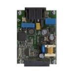


 工商网监
湘ICP备2023018690号
工商网监
湘ICP备2023018690号
