AN3119
Application note
250 W transition-mode PFC pre-regulator with the new L6563S
Introduction
This application note describes a demonstration board based on the new transition-mode
PFC controller L6563S and presents the results of its bench evaluation. The board
implements a 250 W, wide-range mains input PFC pre-conditioner suitable for desktop PCs,
industrial SMPS, flat screen displays, and all SMPS having to meet the IEC61000-3-2 or the
JEITA-MITI standard.
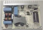
Figure 1.
November 2010
EVL6563S-250W: L6563S 250W TM PFC demonstration board
Doc ID 16849 Rev 2
1/32
www.st.com
�Contents
AN3119
Contents
1
Main characteristics and circuit description . . . . . . . . . . . . . . . . . . . . . 4
2
Electrical diagram . . . . . . . . . . . . . . . . . . . . . . . . . . . . . . . . . . . . . . . . . . . 6
3
Bill of material . . . . . . . . . . . . . . . . . . . . . . . . . . . . . . . . . . . . . . . . . . . . . . 7
4
Test results and significant waveforms . . . . . . . . . . . . . . . . . . . . . . . . 10
4.1
Harmonic content measurement . . . . . . . . . . . . . . . . . . . . . . . . . . . . . . . 10
4.2
MOSFET current, TM signals, and L6563S THD optimizer . . . . . . . . . . . 13
4.3
Voltage feed-forward and brown-out function . . . . . . . . . . . . . . . . . . . . . . 15
4.4
Startup operation . . . . . . . . . . . . . . . . . . . . . . . . . . . . . . . . . . . . . . . . . . . 19
4.5
PFC_OK pin and feedback failure (open-loop) protection . . . . . . . . . . . . 20
4.6
TBO (tracking boost option) . . . . . . . . . . . . . . . . . . . . . . . . . . . . . . . . . . . 22
4.7
Power management and housekeeping functions . . . . . . . . . . . . . . . . . . 23
5
Layout hints . . . . . . . . . . . . . . . . . . . . . . . . . . . . . . . . . . . . . . . . . . . . . . . 25
6
Thermal map . . . . . . . . . . . . . . . . . . . . . . . . . . . . . . . . . . . . . . . . . . . . . . 26
7
EMI filtering and conducted EMI pre-compliance measurements . . . 28
8
References . . . . . . . . . . . . . . . . . . . . . . . . . . . . . . . . . . . . . . . . . . . . . . . . 30
9
Revision history . . . . . . . . . . . . . . . . . . . . . . . . . . . . . . . . . . . . . . . . . . . 31
2/32
Doc ID 16849 Rev 2
�AN3119
List of figures
List of figures
Figure 1.
Figure 2.
Figure 3.
Figure 4.
Figure 5.
Figure 6.
Figure 7.
Figure 8.
Figure 9.
Figure 10.
Figure 11.
Figure 12.
Figure 13.
Figure 14.
Figure 15.
Figure 16.
Figure 17.
Figure 18.
Figure 19.
Figure 20.
Figure 21.
Figure 22.
Figure 23.
Figure 24.
Figure 25.
Figure 26.
Figure 27.
Figure 28.
Figure 29.
Figure 30.
Figure 31.
Figure 32.
Figure 33.
Figure 34.
Figure 35.
Figure 36.
Figure 37.
Figure 38.
Figure 39.
Figure 40.
Figure 41.
Figure 42.
Figure 43.
EVL6563S-250W: L6563S 250W TM PFC demonstration board . . . . . . . . . . . . . . . . . . . . . 1
EVL6563S-250W TM PFC demonstration board: electrical schematic . . . . . . . . . . . . . . . . 6
EVL6563S-250W TM PFC: compliance to EN61000-3-2 standard at 250 W. . . . . . . . . . . 10
EVL6563S-250W TM PFC: compliance to JEITA-MITI standard at 250 W . . . . . . . . . . . . 10
EVL6563S-250W TM PFC: compliance to EN61000-3-2 standard at 70 W. . . . . . . . . . . . 10
EVL6563S-250W TM PFC: compliance to JEITA-MITI standard at 70 W . . . . . . . . . . . . . 10
EVL6563S-250W TM PFC: input current waveform @230 V-50 Hz - 250 W load . . . . . . . 11
EVL6563S-250W TM PFC: input current waveform @100 V-50 Hz - 250 W load . . . . . . . 11
EVL6563S-250W TM PFC: input current waveform @230 V-50 Hz - 70 W load . . . . . . . . 11
EVL6563S-250W TM PFC: input current waveform @100 V-50 Hz - 70 W load . . . . . . . . 11
EVL6563S-250W TM PFC: power factor vs. output power. . . . . . . . . . . . . . . . . . . . . . . . . 12
EVL6563S-250W TM PFC: THD vs. output power . . . . . . . . . . . . . . . . . . . . . . . . . . . . . . . 12
EVL6563S-250W TM PFC: efficiency vs. output power . . . . . . . . . . . . . . . . . . . . . . . . . . 12
EVL6563S-250W TM PFC: average efficiency acc. to ES-2 . . . . . . . . . . . . . . . . . . . . . . . 12
EVL6563S-250W TM PFC: static Vout regulation vs. output power . . . . . . . . . . . . . . . . . 13
EVL6563S-250W TM PFC: MOSFET current at 100 Vac - 50 Hz - full load . . . . . . . . . . . 14
EVL6563S-250W TM PFC: MOSFET current at 100 Vac - 50 Hz - full load . . . . . . . . . . . 14
EVL6563S-250W TM PFC: L6563S control pins-1 at 115 Vac - 60 Hz - full load . . . . . . . 14
EVL6563S-250W TM PFC: L6563S control pins-2 at 115 Vac - 60 Hz - full load . . . . . . . 14
L6562A input mains surge 90 Vac to 140 Vac - no VFF input . . . . . . . . . . . . . . . . . . . . . . 16
EVL6563S-250W TM PFC: input mains surge 90 Vac to 140 Vac . . . . . . . . . . . . . . . . . . . 16
L6562A: input mains dip 140 Vac to 90 Vac - no VFF input . . . . . . . . . . . . . . . . . . . . . . . . 16
EVL6563S-250W TM PFC: input mains dip 140 Vac to 90 Vac . . . . . . . . . . . . . . . . . . . . . 16
L6563 Input current at 100 Vac -50Hz CFF=0.47 µF, RFF=390 kW . . . . . . . . . . . . . . . . . 17
EVL6563S-250W TM PFC: input current at 100 Vac -50 Hz CFF=1 µF, RFF=1 MW . . . . 17
EVL6563S-250W TM PFC: startup attempt at 80 Vac-60 Hz - full load . . . . . . . . . . . . . . . 18
EVL6563S-250W TM PFC: startup with slow input voltage increasing - full load. . . . . . . . 18
EVL6563S-250W TM PFC: turn-off with slow input voltage decreasing - full load . . . . . . . 18
EVL6563S-250W TM PFC: startup at 90 Vac-60 Hz - full load . . . . . . . . . . . . . . . . . . . . . 19
EVL6563S-250W TM PFC: startup at 265 Vac-50 Hz - full load . . . . . . . . . . . . . . . . . . . . 19
EVL6563S-250W load transient at 115 Vac - 60 Hz - full load to no-load . . . . . . . . . . . . . 21
EVL6563S-250W TM PFC: open-loop at 115 Vac - 60 Hz - full load . . . . . . . . . . . . . . . . . 21
EVL6563S-250W TM PFC: open-loop at 115 Vac - 60 Hz - full load - long acquisition . . . 21
L6563S on/off control by a cascaded converter controller via the PFC_OK or RUN pin . . 23
Interface circuits that let the L6563S switch on or off a PWM controller - not latched . . . . 24
Interface circuits that let the L6563S switch on or off a PWM controller - latched . . . . . . . 24
EVL6563S-250W TM PFC: PCB layout (SMT side view) . . . . . . . . . . . . . . . . . . . . . . . . . . 25
Thermal map at 115 Vac - 60 Hz - full load - PCB top side . . . . . . . . . . . . . . . . . . . . . . . . 26
Thermal map at 230 Vac - 50 Hz - full load - PCB top side . . . . . . . . . . . . . . . . . . . . . . . . 26
EVL6563S-250W CE AVG measurement at 115 Vac-60 Hz - full load - phase wire . . . . . 28
EVL6563S-250W CE AVG measurement at 115 Vac-60 Hz - full load - neutral wire . . . . 28
EVL6563S-250W CE AVG measurement at 230 Vac-50 Hz - full load - phase wire . . . . . 29
EVL6563S-250W CE AVG measurement at 230 Vac-50 Hz - full load - neutral wire . . . . 29
Doc ID 16849 Rev 2
3/32
�Main characteristics and circuit description
1
AN3119
Main characteristics and circuit description
The main characteristics of the SMPS are:
●
Line voltage range: 90 to 265 Vac
●
Line frequency (fL): 47 to 63 Hz
●
Regulated output voltage: 400 V
●
Rated output power: 250 W
●
Maximum 2fL output voltage ripple: 20 V pk-pk
●
Hold-up time: 10 ms (VDROP after hold-up time: 300 V)
●
Minimum switching frequency: 40 kHz
●
Minimum estimated efficiency: 93 % (@Vin=90 Vac, Pout=250 W)
●
Maximum ambient temperature: 50 °C
●
PCB type and size: single side, 35 µm, CEM-1, 88 x 116 mm
This demonstration board implements a power factor correction (PFC) pre-regulator, 250 W
continuous power, delivering a regulated 400 V rail from a wide range mains voltage and
providing for the reduction of the mains harmonics, allowing the European EN61000-3-2 or
the Japanese JEITA-MITI standard to be met. The regulated output voltage is typically the
input for the cascaded isolated DC-DC converter which provides the output rails required by
the load.
The power stage of the PFC is a conventional boost converter, connected to the output of
the D1 rectifier bridge. It is completed by the L2 coil, the D3 diode and the C5 capacitor. The
boost switch is represented by the Q1 and Q2 power MOSFETs, connected in parallel. The
NTC R1 limits the inrush current at switch-on. It has been connected on the DC rail, in
series to the output electrolytic capacitor, in order to improve the efficiency during low-line
operation. In fact the RMS current flowing into the output stage is lower than current flowing
into the input stage at the same input voltage. The board is equipped with an input EMI filter
necessary to filter the switching noise coming from the boost stage.
At startup the L6563S is powered by the capacitor C9 which is charged via the R5 and R11
resistors. The L2 secondary winding and the charge pump circuit (C6, R2, D4 and D5)
generate the Vcc voltage powering the L6563S during normal operations. The L2 secondary
winding is also connected to the L6563S pin #11 (ZCD) through the R14 resistor. Its
purpose is to supply the information that L2 has demagnetized, needed by the internal logic
to trigger a new switching cycle.
The R4, R8, R12, and R15 divider provides, to the L6563S multiplier, the information for the
instantaneous mains voltage which is used to modulate the peak current of the boost.
The R3, R6, R7 with R9 and R10 resistors are dedicated to sensing the output voltage and
giving the feedback information necessary to the L6563S to regulate the output voltage. The
C7, R13 and C10 components are the error amplifier compensation network necessary to
obtain the required loop stability.
The peak current is sensed by the R23 and R24 resistors in series to the MOSFET and the
signal is fed into pin #4 (CS) of the L6563S via the filter by R20 and C14.
C12, R27 and R28 are connected to pin #5 (VFF), they complete an internal peak-holding
circuit which obtains the information on the RMS mains voltage. The voltage signal at this
pin, a DC level equal to the peak voltage on pin #3 (MULT), is fed to a second input to the
multiplier for 1/V2 function necessary to compensate the control loop gain dependence on
4/32
Doc ID 16849 Rev 2
�AN3119
Main characteristics and circuit description
the mains voltage. Additionally, pin #10 (RUN) is connected to pin# 5 (VFF) through the R27
and R28 resistor divider, providing a voltage level for brown-out (AC mains under voltage)
protection. A voltage on the RUN pin below 0.8 V shuts down (not latched) the IC and brings
its consumption to a considerably lower level. The L6563S restarts as the voltage at the pin
rises above 0.88 V.
The R21, R25, R26 and R33 dividers provide the information regarding the output voltage
level to the L6563S pin #7 (PFC_OK). It is required by the L6563S output voltage monitoring
and disable functions used for PFC protection purposes.
If the voltage on pin #7 exceeds 2.5 V the IC stops switching and restarts as the voltage on
the pin falls below 2.4 V, realizing the so-called dynamic OVP, preventing the output voltage
becoming excessive in case of transient, due to the slow response of the error amplifier.
However, if contemporaneously the voltage of the INV pin falls below 1.66 V (typ.), a
feedback failure is assumed. In this case the device is latched off. Normal operation can be
resumed only by cycling Vcc, bringing its value lower than 6 V, before moving up to turn-on
the threshold.
Additionally, if the voltage on pin #7 (PFC_OK) is tied below 0.23 V, the L6563S is shut
down. To restart the L6563S operation the voltage on pin #7 (PFC_OK) must increase
above 0.27 V. This function can be used as a remote on/off control input.
To allow the interfacing of the board with a D2D converter the J3 connector allows the
powering of the L6563S with an external Vcc. It also gives the opportunity to manage failure
or abnormal conditions via the PWM_LATCH (#8) and PWM_STOP (#9) pins. The L6563S
operation can also be disabled or enabled to properly manage light load or failure conditions
by the D2D via the PFC_OK pin (#7), still available at pin #5 of J3 (on/off). For further details
please see Section 4.7.
Doc ID 16849 Rev 2
5/32
�Doc ID 16849 Rev 2
&��
�X)
&��
�1�
5��
�0�
5��
��.
5;�
�5�
5��
�0�
5�
�0�
5�
�0�
&��
���S)
5��
��.
&�
��1
&��
�1�
&��
���1
5��
���.
3&%�5(9���
=�
������9DF
�
�
�
�
�
�
�
�
�
,19
3)& �2.
7%2
9))
&6
08/7
&203
581
=&'
*1'
*'
9&&
5��
��.
�
�
��
��
��
-3;�
�5�
5;�
���1
&�
-3;�
-3�
:,5(�-803(5
3:0�/$7&+
��
��
5��
���.
5�
���.
/+�������@
3RZHU�)DFWRU
����
�����
�����
����
����
3RXW� ��:
3RXW� ���:
3RXW� ���:
�����
3RXW� ���:
3RXW� ��:
2XWSXW�3RZHU
3RXW� ���:
3RXW� ���:
2XWSXW�3RZHU
!-�����V�
3RXW� ���:
!-�����V�
The measured efficiency is shown in Figure 13, measured according to the ES-2
requirements. It is excellent at all load and line conditions; at full load it is always higher than
94 %, making this design suitable for high efficiency power supply. The average efficiency
calculated according to the ES-2 requirements at different nominal mains voltages is shown
in Figure 14.
Figure 13. EVL6563S-250W TM PFC:
efficiency vs. output power
Figure 14. EVL6563S-250W TM PFC: average
efficiency acc. to ES-2
$YHUDJH�(IILFLHQF\�DFF��WR�(6��
(IILFLHQF\�YV��2XWSXW�3RZHU
���
���
$9*�(II��#���9DF���+]
���
$9*�(II��#���9DF���+]
$9*�(IILFLHQF\�>�@
(IILFLHQF\�>�@
���
���
���
���
���
(II��#���9DF���+]
���
���
���
���
(II��#���9DF���+]
���
(II��#���9DF���+]
���
���
3RXW� ��:
3RXW� ���:
3RXW� ���:
3RXW� ���:
2XWSXW�3RZHU
9LQBDF�>9UPV@
$&�LQSXW�YROWDJH
!-�����V�
12/32
$9*�(II��#���9DF���+]
Doc ID 16849 Rev 2
!-�����V�
�AN3119
Test results and significant waveforms
Figure 15. EVL6563S-250W TM PFC: static Vout regulation vs. output power
�����
2XWSXW�9ROWDJH�YV��2XWSXW�3RZHU
�����
9RXW�>9GF@
�����
�����
�����
�����
9RXW�#���9DF���+]
�����
9RXW�#���9DF���+]
�����
9RXW�#���9DF���+]
�����
3RXW� ��:
3RXW� ���:
3RXW� ���:
3RXW� ���:
2XWSXW�3RZHU
!-�����V�
The measured output voltage at different line and static load conditions is shown in
Figure 15. As seen, the voltage is very stable over all the input voltage and output load
range.
4.2
MOSFET current, TM signals, and L6563S THD optimizer
In the following images the waveforms relevant to the switch current at 100 Vac voltage
mains are shown; in Figure 16 and 17 it can be noted that the current peaks in the two
MOSFETs in parallel are very close to each other, demonstrating the perfect current sharing
between the two devices. The two MOSFETs in parallel allow the total thermal resistance
junction-heat sink to decrease, therefore the same peak current can be managed using two
smaller and cheaper MOSFETs instead of a bigger one.
In Figure 16, close to the zero crossing points of the sinewave, it is possible to note the
action of the THD optimizer embedded in the L6563S. It is a circuit which minimizes the
conduction dead-angle occurring at the AC input current near the zero-crossings of the line
voltage (crossover distortion). In this way, the THD (total harmonic distortion) of the current
is considerably reduced. A major cause of this distortion is the inability of the system to
transfer energy effectively when the instantaneous line voltage is very low. This effect is
magnified by the high frequency filter capacitor placed after the bridge rectifier, which
retains some residual voltage causing the diodes of the bridge rectifier to be reverse-biased
and the input current flow to temporarily stop. To overcome this issue the device forces the
PFC pre-regulator to process more energy near the line voltage zero-crossings as
compared to that commanded by the control loop. This results in both minimizing the time
interval where energy transfer is lacking and fully discharging the high-frequency filter
capacitor after the bridge. Essentially, the circuit artificially increases the on-time of the
power switch with a positive offset added to the output of the multiplier in the proximity of the
line voltage zero-crossings. This offset is reduced as the instantaneous line voltage
increases, so that it becomes negligible as the line voltage moves towards the top of the
sinusoid. Furthermore, the offset is modulated by the voltage on the VFF pin so as to have
as little offset at low-line, where energy transfer at zero crossings is typically quite good, and
a larger offset at high-line where the energy transfer gets worse.
To achieve maximum benefit from the THD optimizer circuit, the high-frequency filter
capacitors after the bridge rectifier should be minimized, maintaining compatibility with EMI
Doc ID 16849 Rev 2
13/32
�Test results and significant waveforms
AN3119
filtering needs. In fact, a large capacitance introduces a conduction dead-angle of the AC
input current in itself, therefore reducing the effectiveness of the optimizer circuit.
Figure 16. EVL6563S-250W TM PFC: MOSFET Figure 17. EVL6563S-250W TM PFC: MOSFET
current at 100 Vac - 50 Hz - full load
current at 100 Vac - 50 Hz - full load
CH1: Q1 gate voltage, CH2: Q2 gate voltage,
CH1: Q1 gate voltage, CH2: Q2 gate voltage
CH3: Q1 drain current
CH3: Q1 drain current
CH4: Q2 drain current
CH4: Q2 drain current
In Figure 18 the detail of the waveforms at switching frequency shows the operation of the
transition mode control; once the inductor has transferred all the energy stored, a falling
edge on the ZCD pin (#11) is detected and it triggers a new on-time by setting the gate drive
high. Once the current signal on the CS pin (#4) has reached the level programmed by the
internal multiplier circuitry, according to the input mains instantaneous voltage and the error
amplifier output level, the gate drive is set low and MOSFET conduction is stopped. During
the following off-time the energy stored in the inductor is transferred into the output capacitor
and to the load. At the end of the current conduction a new demagnetization is detected by
the ZCD which provides for a new on-time of the MOSFET.
In Figure 19 the waveforms of the MULT, VFF, INV, and COMP pins are shown.
Figure 18. EVL6563S-250W TM PFC: L6563S
control pins-1 at 115 Vac - 60 Hz full load
Figure 19. EVL6563S-250W TM PFC: L6563S
control pins-2 at 115 Vac - 60 Hz full load
CH1: GD - pin #13, CH2: ZCD - pin #11, CH3: CS - pin #4
CH1: INV - pin #1, CH2: MULT - pin #3, CH3: COMP - pin #2
CH4: MULT - pin #3
CH4: VFF - pin #5
14/32
Doc ID 16849 Rev 2
�AN3119
4.3
Test results and significant waveforms
Voltage feed-forward and brown-out function
The power stage gain of PFC pre-regulators varies with the square of the RMS input
voltage. As does the crossover frequency fc of the overall open-loop gain because the gain
has a single pole characteristic. This leads to large trade-offs in the design. For example,
setting the gain of the error amplifier to get fc = 20 Hz @ 264 Vac means having fc = 4 Hz @
88 Vac, resulting in sluggish control dynamics. Additionally, the slow control loop causes
large transient current flow during rapid line or load changes that are limited by the
dynamics of the multiplier output. This limit is considered when selecting the sense resistor
to let the full load power pass under minimum line voltage conditions, with some margin. But
a fixed current limit allows excessive power input at high line, whereas a fixed power limit
requires the current limit to vary inversely with the line voltage.
Voltage feed-forward can compensate for the gain variation with the line voltage and allow
all of the above-mentioned issues to be overcome. It consists of deriving a voltage
proportional to the input RMS voltage, feeding this voltage into a squarer/divider circuit (1/V2
corrector) and providing the resulting signal to the multiplier which generates the current
reference for the inner current control loop.
In this way a change of the line voltage causes an inversely proportional change of the halfsine amplitude at the output of the multiplier (if the line voltage doubles the amplitude of the
multiplier output is halved and vice versa) so that the current reference is adapted to the new
operating conditions with (ideally) no need for invoking the slow dynamics of the error
amplifier. Additionally, the loop gain is constant throughout the input voltage range, which
significantly improves dynamic behavior at low-line and simplifies loop design.
In fact, with other PFC embedding the voltage feed-forward, deriving a voltage proportional
to the RMS line voltage implies a form of integration, which has its own time constant. If it is
too small the voltage generated is affected by a considerable amount of ripple at twice the
mains frequency which causes distortion of the current reference (resulting in high THD and
poor PF); if it is too large there is a considerable delay in setting the right amount of feedforward, resulting in excessive overshoot and undershoot of the pre-regulator's output
voltage in response to large line voltage changes. Clearly a trade-off was required.
The L6563S realizes an innovative voltage feed-forward which both surges and drops, with a
technique that overcomes the time constant trade-off issue whichever voltage change
occurs on the mains. A CFF (C12) capacitor and an RFF (R27 + R28) resistor, both
connected to the VFF pin (#5), complete an internal peak-holding circuit that provides a DC
voltage equal to the peak of the rectified sinewave applied on the MULT pin (#3). In this way,
in the case of sudden line voltage rise, CFF is rapidly charged through the low impedance of
the internal diode; in the case of line voltage drop, an internal “mains drop” detector enables
a low impedance switch which suddenly discharges CFF, avoiding a long settling time before
reaching the new voltage level. Consequently, an acceptably low steady-state ripple and low
current distortion can be achieved without any considerable undershoot or overshoot on the
preregulator's output, as in systems with no feed-forward compensation.
In Figure 21 the behavior of the EVL6563S-250W demonstration board in the case of an
input voltage surge from 90 to 140 Vac is shown; in the image it is evident that the VFF
function provides for the stability of the output voltage which is not affected by the input
voltage surge. In fact, thanks to the VFF function, the compensation of the input voltage
variation is very fast and the output voltage remains stable at its nominal value. The
opposite is confirmed in Figure 20; the behavior of a PFC using the L6562A and delivering
the same output power is shown; in the case of a mains surge the controller cannot
compensate and output voltage stability is guaranteed only by the feedback loop.
Unfortunately, as previously mentioned, its bandwidth is narrow and therefore the output
Doc ID 16849 Rev 2
15/32
�Test results and significant waveforms
AN3119
voltage has a significant deviation from the nominal value. The circuit has the same behavior
in the case of mains surge at any input voltage, and it is not affected even if the input mains
surge happens at any point of the input sinewave.
Figure 20. L6562A input mains surge 90 Vac to Figure 21. EVL6563S-250W TM PFC: input
140 Vac - no VFF input
mains surge 90 Vac to 140 Vac
CH1: Vout, CH2: MULT (pin #3), CH4: I_AC
CH1: Vout, CH3: VFF (pin #5), CH2: MULT (pin #3)
CH4: I_AC
In Figure 23 the circuit behavior in the case of mains dip is shown; as previously described,
the internal circuitry has detected the decreasing of the mains voltage and it has activated
the CFF internal fast discharge. As seen, in this case the output voltage changes but in a few
mains cycles it comes back to the nominal value. The situation is different if we compare it
with the performance of a controller without the VFF function. In Figure 22 the behavior of a
PFC using the L6562A and delivering similar output power is shown; in the case of a mains
dip from 140 Vac to 90 Vac the output voltage variation is not very different but the output
voltage requires a longer time to restore the original value. In tests with a wider voltage
variation (e.g. 265 Vac to 90 Vac) the output voltage variation of a PFC without the voltage
feed-forward fast discharging is far more emphasized.
Figure 22. L6562A: input mains dip 140 Vac to Figure 23. EVL6563S-250W TM PFC: input
90 Vac - no VFF input
mains dip 140 Vac to 90 Vac
CH1: Vout, CH2: MULT (pin #3), CH4: I_AC
CH1: Vout, CH2: MULT (pin #3), CH2: VFF (pin #5)
CH4: I_AC
16/32
Doc ID 16849 Rev 2
�AN3119
Test results and significant waveforms
It is also possible to see, comparing Figure 24 and Figure 25, that the input current of the
latter has a better shape and the 3rd harmonic current distortion is not noticeable; this
demonstrates the benefits of the new voltage feed-forward circuit integrated into the
L6563S, allowing a fast response to mains disturbances but using a quite long VFF time
constant, also providing very low THD and high PF at the same time, as confirmed by the
measurements below in Figure 24 and 25:
Figure 24. L6563 Input current at 100 Vac 50Hz CFF=0.47 µF, RFF=390 kΩ
Figure 25. EVL6563S-250W TM PFC: input
current at 100 Vac -50 Hz CFF=1 µF,
RFF=1 MΩ
THD= 4.36%, 3rd harmonic=94.6 mA
THD= 2.94%, 3rd harmonic=30.5 mA
CH2: MULT (pin #3)
CH2: MULT (pin #3)
CH3: VFF (pin #5)
CH3: VFF (pin #5)
CH4: I_AC
CH4: I_AC
Another function offered by the L6563S is brown-out protection, which is basically a notlatched shutdown function which must be activated when a mains under voltage condition is
detected. This abnormal condition may cause overheating of the primary power section due
to an excess of RMS current. Brown-out can also cause the PFC pre-regulator to work
open-loop and this could be dangerous to the PFC stage itself and the downstream
converter, should the input voltage return abruptly to its rated value. A further problem is the
spurious restarts which may occur during converter power-down and that cause the output
voltage of the converter not to decay to zero monotonically. For these reasons it is usually
preferable to shut down the device in the case of brown-out.
Brown-out function is done by sensing the input mains through an internal comparator
connected to RUN (pin #10), connected via a divider to VFF (pin #5) which delivers a voltage
signal proportional to the input mains. The enable and disable thresholds at which the
L6563S starts or stops the operation can be adjusted modifying that divider ratio. For
additional information please see [2].
Doc ID 16849 Rev 2
17/32
�Test results and significant waveforms
AN3119
Figure 26. EVL6563S-250W TM PFC: startup attempt at 80 Vac-60 Hz - full load
CH1: PFC output voltage
CH2: Vcc voltage (pin #14)
CH3: RUN (pin #10)
CH4: gate drive (pin #13)
In Figure 26 a startup tentative below the threshold is shown. As seen, at startup the RUN
pin does not allow the PFC startup even if the Vcc has reached the turn-on threshold. PFC
output voltage remains at the peak of the input sinewave.
In Figure 27 and 28 the waveforms of the circuit during operation of brown-out protection are
shown. In both cases the mains voltage was increased or decreased slowly; as seen, both
at turn-on or turn-off there are no bouncing or starting attempts by the PFC converter.
Figure 27. EVL6563S-250W TM PFC: startup
Figure 28. EVL6563S-250W TM PFC: turn-off
with slow input voltage increasing with slow input voltage decreasing
full load
- full load
CH1: PFC output voltage
CH1: PFC output voltage
CH2: gate drive (pin #13)
CH2: gate drive (pin #13)
CH3: RUN (pin #10)
CH3: RUN (pin #10)
CH4: PWM_stop (pin #9)
CH4: PWM_stop (pin #9)
18/32
Doc ID 16849 Rev 2
�AN3119
4.4
Test results and significant waveforms
Startup operation
Figure 29 and 30 show the waveforms during the startup of the circuit at mains plug-in.
The R5 and R11 startup resistors charge the Vcc C9 capacitor, therefore Vcc voltage rises
up to the turn-on threshold, and the L6563S starts operating. For a short time the energy is
supplied by the Vcc capacitor, and then the auxiliary winding with the charge pump circuit
takes over.
Because the startup resistors are always connected to the mains, their power consumption
during normal operation might affect the efficiency of the power supply once it operates at
light load. Therefore the value of the startup resistors must be found as a compromise
between the startup time at minimum input mains and the power dissipation at maximum
input mains.
In Figure 28 and 29 the waveforms during startup of the circuit at mains plug-in are shown.
Notice that because the Vcc voltage rise depends on the input voltage, the wake-up time is
dependent on the input mains voltage.
The same figures show that the output voltage rises from the peak value of the rectified
mains to the nominal value of the PFC output voltage and the good phase margin of the
compensation network allows a clean startup without overshoot.
Figure 29. EVL6563S-250W TM PFC: startup at Figure 30. EVL6563S-250W TM PFC: startup at
90 Vac-60 Hz - full load
265 Vac-50 Hz - full load
CH1: PFC output voltage
CH1: PFC output voltage
CH2: Vcc voltage (pin #14)
CH2: Vcc voltage (pin #14)
CH3: RUN (pin #10)
CH3: RUN (pin #10)
CH4: gate drive (pin #13)
CH4: gate drive (pin #13)
Doc ID 16849 Rev 2
19/32
�Test results and significant waveforms
4.5
AN3119
PFC_OK pin and feedback failure (open-loop) protection
During normal operation, the voltage control loop provides for the output voltage (Vout) of
the PFC pre-regulator close to its nominal value, set by the resistors ratio of the feedback
output divider. In the L6563S the PFC_OK pin (#7) has been dedicated to monitoring the
output voltage with a separate resistor divider made up of R21, R25, R26 (high) and R33
(low), see Figure 2. This divider is selected so that the voltage at the pin reaches 2.5 V if the
output voltage exceeds a pre-set value (VOVP), usually larger than the maximum Vout that
can be expected, also including worst-case load/line transients.
For the EVL6563S-250W:
Vo = 400 V, Vovp = 434 V. Select: R21+R25+R26=8.8 MΩ; then:
R33=8.8 MΩ·2.5/(434-2.5)=51 kΩ.
Once this function is triggered, the gate drive activity is immediately stopped until the
voltage on the PFC_OK pin drops below 2.4 V. An example is given in Figure 31. Notice that
both feedback dividers connected to the L6563S pin (#1) and PFC_OK pin (#7) can be
selected without any constraints. The unique criterion is that both dividers have to sink a
current from the output bus which needs to be significantly higher than the current biasing
the Error amplifier and PFC_OK comparator.
The OVP function described above is able to handle “normal” over voltage conditions, i.e.
those resulting from an abrupt load/line change or occurring at startup. In a case where the
overvoltage is generated by a feedback disconnection, for instance, when one of the upper
resistors of the output divider fails to open, an additional circuitry detects the voltage drop of
the INV pin. If the voltage on pin INV is lower than 1.66 V and at the same time the OVP is
active, a feedback failure is assumed. Therefore, the gate drive activity is immediately
stopped, the device is shut down, its quiescent consumption is reduced below 180 µA and
the condition is latched as long as the supply voltage of the L6563S is above the UVLO
threshold. To restart the system it is necessary to recycle the input power, so that the Vcc
voltage of the L6563S goes below Vccrestart. Note that this function offers complete
protection against not only feedback loop failures or erroneous settings, but also against a
failure of the protection itself. Either resistor of the PFC_OK divider failing (short or open), or
a PFC_OK pin floating, results in shutting down the IC and stopping the pre-regulator.
Moreover, the PFC_OK pin doubles its function as a not-latched IC disable; a voltage below
0.23 V shuts down the IC, reducing its consumption to below 2 mA. To restart the IC simply
let the voltage at the pin go above 0.27 V.
20/32
Doc ID 16849 Rev 2
�AN3119
Test results and significant waveforms
Figure 31. EVL6563S-250W load transient at 115 Vac - 60 Hz - full load to no-load
CH1: PFC output voltage,
CH2: PFC_OK (pin #7),
CH3: gate drive (pin #13),
CH4: Iout
The event of an open-loop is demonstrated in Figure 32 and 33; notice the protection
intervention, latching the operation of the L6563S. As mentioned previously, to restart the
system it is necessary to recycle the input power. The connection of the startup resistors
after the rectifier bridge allows a restart, in case of latch, faster than connecting the resistor
to the bulk capacitor. In this case, to restart the operation it is necessary to wait the time
needed to discharge the bulk capacitor below the Vccrestart to reset the latch and then
resume the operation.
Figure 32. EVL6563S-250W TM PFC: openloop at 115 Vac - 60 Hz - full load
Figure 33. EVL6563S-250W TM PFC: openloop at 115 Vac - 60 Hz - full load long acquisition
CH1: PFC output voltage
CH1: PFC output voltage
CH2: Vcc (pin #14)
CH2: Vcc (pin #14)
CH3: gate drive (pin #13)
CH3: gate drive (pin #13)
CH4: PWM_LATCH (pin#8)
CH4: PWM_LATCH (pin#8)
Doc ID 16849 Rev 2
21/32
�Test results and significant waveforms
4.6
AN3119
TBO (tracking boost option)
To achieve the TBO function on the L6563S a dedicated input of the multiplier is available on
pin #6 (TBO); the function can be realized by simply connecting a resistor (RT) between the
TBO pin and ground.
Usually, in traditional PFC stages, the DC output voltage is regulated at a fixed value
(typically 400 V) but in some applications it may be advantageous to regulate the PFC
output voltage with the “tracking boost” or “follower boost” approach. In this way the circuit
with TBO function provides better efficiency, and thanks to the lower differential voltage
across the boost inductor the value of L2 can be reduced, compared to the same circuit
without TBO function.
The TBO pin presents a DC level equal to the peak of the MULT pin voltage and is then
representative of the mains RMS voltage. The resistor defines a current, equal to
V(TBO)/RT, which is internally 1:1 mirrored and sunk from the INV pin (#1) input of the error
amplifier. In this way, when the mains voltage increases, the voltage at the TBO pin also
increases, as does the current flowing through the resistor connected between TBO and
GND. Then a larger current is sunk by the INV pin and the output voltage of the PFC preregulator is forced higher. Obviously the output voltage moves in the opposite direction if the
input voltage decreases.
To avoid an undesired output voltage rise, should the mains voltage exceed the maximum
specified value, the voltage at the TBO pin is clamped at 3 V. By properly selecting the
multiplier bias it is possible to set the maximum input voltage above which input-to-output
tracking ends and the output voltage becomes constant. If this application is not used and
the pin is left open, the device regulates at a fixed output voltage.
22/32
Doc ID 16849 Rev 2
�AN3119
4.7
Test results and significant waveforms
Power management and housekeeping functions
A special feature of the L6563S is that it facilitates the implementation of the “housekeeping”
circuitry needed to coordinate the operation of the PFC stage to that of the cascaded DCDC converter. The functions realized by the housekeeping circuitry ensure that transient
conditions like power-up or power-down sequencing or failures of either power stage be
properly handled. The L6563S provides some pins to do that.
As already mentioned, one communication line between the L6563S and the PWM
controller of the cascaded DC-DC converter is the PWM_LATCH (pin #8), which is normally
open when the PFC works properly. It goes high if the L6563S loses control of the output
voltage (because of a failure of the control loop) or if the boost inductor saturates, with the
aim of also latching off the PWM controller of the cascaded DC-DC converter.
A second communication line can be established via the disable function included in the
RUN pin. Typically, this line is used to allow the PWM controller of the cascaded DC-DC
converter to shut down the L6563S in the case of light load, to minimize the no-load input
consumption of the power supply.
Examples of intefacing some ST half-bridges controllers are shown in Figure 34.
Figure 34. L6563S on/off control by a cascaded converter controller via the PFC_OK
or RUN pin
�
�
0&#?34/0
�
,����! �
�
�
0&#?34/0
�
,���� �
� ��
�25. � ��� �
,����3
0&#?/+
� ��
�25. � ��� �
,����3
�
0&#?/+
�
!-�����V�
The third communication line is the PWM_STOP pin (# 9), which works in conjunction with
the RUN pin (#10). The purpose of the PWM_STOP pin is to inhibit the PWM activity of both
the PFC stage and the cascaded DC-DC converter. The pin is an open collector, normally
open, that goes low if the device is disabled by a voltage lower than 0.8 V on the RUN pin
(#10). It is important to point out that this function works correctly in systems where the PFC
stage is the master and the cascaded DC-DC converter is the slave or, in other words,
where the PFC stage starts first, powers both controllers and enables/disables the operation
of the DC-DC stage. This function is quite flexible and can be used in different ways. In
systems comprising an auxiliary converter and a main converter (e.g. desktop PC's, silver
box or high end flat-TVs, and monitors), where the auxiliary converter also powers the
controllers of the main converter, the RUN pin (#10) can be used to start and stop the main
converter. In the simplest case, to enable/disable the PWM controller the PWM_STOP pin
(#9) can be connected to either the output of the error amplifier or, if provided the chip, to the
soft-start pin.
The EVL6563S-250W offers the possibility to test these function by connecting it to the
cascaded converter via the R30, R31, R32 series resistors. Regarding the PWM_STOP pin
Doc ID 16849 Rev 2
23/32
�Test results and significant waveforms
AN3119
(#9), which is an open collector type, if it needs a pull-up resistor please connect it close to
the cascaded PWM for a better noise immunity.
Figure 35. Interface circuits that let the L6563S Figure 36. Interface circuits that let the L6563S
switch on or off a PWM controller switch on or off a PWM controller not latched
latched
/.
/&&
�
�
25.
�
,�����!�8��OR�
5#���X�8��
5#���X�8��
,����� 8��OR�
,�����8��OR��
,����!�8��OR�
,����!�"�8���
�
��
�
,����3
07-�2%3
CONTROLLER �
�
�
8
,����3�
07-?34/0
�
,�����!�8���
,�����8��
,����!�8��
,����!�"�8��
!-�����V�
24/32
Doc ID 16849 Rev 2
07-�2%3
CONTROLLER �
� 07-?,!4# (
�
8
�
!-�����V�
�AN3119
5
Layout hints
Layout hints
The layout of any converter is a very important phase in the design process needing as
much attention by the design engineers as any other design phase. Even if it the layout
phase can sometimes look time consuming a good layout surely saves time during the
functional debugging and the qualification phases. Additionally, a power supply circuit with a
correct layout needs smaller EMI filters or less filter stages and so it allows a consistent
money saving.
Converters using the L6563S do not need any special or specific layout rule to be followed;
just the general layout rules for any power converter have to be applied carefully. Basic rules
are listed below; they can be used for other PFC circuits having any power level, working
either in transition mode or with a fixed-off time control.
1.
Keep power and signal RTN separated. Connect the return pins of the components
carrying high current such as input filters, sense resistors, or output capacitors, as
close as possible. This point is the RTN star point. A downstream converter must be
connected to this return point.
2.
Minimize the length of the traces relevant to the boost inductor, MOSFET drain, boost
rectifier and output capacitor.
3.
Keep signal components as close as possible to each L6563S relevant pin. To be more
precise, keep the tracks relevant to the pin #1 (INV) net as short as possible.
Components and traces relevant to the Error Amplifier have to be placed far from traces
and connections carrying signals with high dV/dt, such as the MOSFET drain. For high
power converters or very compact PCB layout a 10 nF capacitor connected to pin #9
(PWM_LATCH) and pin #12 (GND) might be required to decrease the noise picked up
by this pin while it is in its high impedance status.
4.
Please connect heat sinks to power GND.
5.
Add an external shield to the boost inductor and connect it to power GND.
6.
Please connect the RTN of signal components including the feedback, PFC_OK, and
MULT dividers close to the L6563S pin #12 (GND).
7.
Connect a ceramic capacitor (100÷470 nF) to pin #14 (Vcc) and pin #12 (GND), close
to the L6563S. Connect this point to the RTN star point (see rule 1).
Figure 37. EVL6563S-250W TM PFC: PCB layout (SMT side view)
Doc ID 16849 Rev 2
25/32
�Thermal map
6
AN3119
Thermal map
In order to check the design reliability, a thermal mapping by means of an IR camera was
done. In Figure 38 the thermal measurements of the board, component side at nominal
input voltage, are shown. Some pointers visible in the image have been placed across key
components or components showing high temperature. The ambient temperature during
both measurements was 27 °C. It is possible to see that the PFC part has a different
temperature depending on the input mains.
Figure 38. Thermal map at 115 Vac - 60 Hz - full load - PCB top side
Figure 39. Thermal map at 230 Vac - 50 Hz - full load - PCB top side
26/32
Doc ID 16849 Rev 2
�AN3119
Thermal map
Table 2.
Thermal maps reference points - PCB top side
Point
Reference
Description
A
D1
Bridge rectifier
B
Q1
PFC MOSFET
C
Q2
PFC MOSFET
D
R1
NTC thermistor
E
R23 and R24
Sense resistors
F
D3
PFC boost rectifier
G
L1
EMI filtering inductor
H
L2
PFC inductor - core
I
L2
PFC inductor - winding
Doc ID 16849 Rev 2
27/32
�EMI filtering and conducted EMI pre-compliance measurements
7
AN3119
EMI filtering and conducted EMI pre-compliance
measurements
Figures 40, 41, 42, and 43 show the measurement in average mode of the conducted noise
at full load and nominal mains voltages for both mains lines. The limits shown in the
diagrams are EN55022 class-B which is the most popular standard for domestic equipment
using a two-wire mains connection.
It is worth remembering that typically a PFC produces a significant differential mode noise
with respect to other topologies. In case an additional margin, with respect to the limits, is
needed, increasing the differential attenuation by increasing the across the line (X)
capacitors or theC4 capacitor after the rectifier bridge is suggested. Sometimes a differential
mode coil connected as a pi-filter placed after, between the bridge rectifier and the boost
stage, is more effective and cheaper than increasing the size of the common mode filter coil
which would filter the differential mode noise by the leakage inductance only between the
two windings.
To recognize if the circuit is affected by common mode or differential mode noise it is
sufficient to compare the spectrum of phase and neutral line measurements; if the two
measurements are very similar the noise is almost totally common mode. If there is a
significant difference between the two measurement spectrums, their difference represents
the amount of differential mode noise. Of course to get a reliable comparison the two
measurements have to be done under the same conditions.
Because the differential mode produces common mode noise through the magnetic field
induced by the current, decreasing the differential mode consequently limits the latter.
As visible in the diagrams, in all test conditions there is at least a 6dB margin of the
measurements with respect to the limits. The measurements have been done in AVG
detection to evaluate the benefit of the jittering effect of the TM control.
Figure 40. EVL6563S-250W CE AVG
Figure 41. EVL6563S-250W CE AVG
measurement at 115 Vac-60 Hz - full
measurement at 115 Vac-60 Hz - full
load - phase wire
load - neutral wire
28/32
Doc ID 16849 Rev 2
�AN3119
EMI filtering and conducted EMI pre-compliance measurements
Figure 43. EVL6563S-250W CE AVG
Figure 42. EVL6563S-250W CE AVG
measurement at 230 Vac-50 Hz - full
measurement at 230 Vac-50 Hz - full
load - phase wire
load - neutral wire
Doc ID 16849 Rev 2
29/32
�References
8
30/32
AN3119
References
1.
L6563S datasheet
2.
AN3027 “How to design a TM PFC pre-regulator with L6563S and L6563H”
Doc ID 16849 Rev 2
�AN3119
9
Revision history
Revision history
Table 3.
Document revision history
Date
Revision
Changes
29-Jun-2010
1
Initial release.
24-Nov-2010
2
Update Chapter 1 on page 4, Chapter 4.5 on page 20.
Doc ID 16849 Rev 2
31/32
�AN3119
Please Read Carefully:
Information in this document is provided solely in connection with ST products. STMicroelectronics NV and its subsidiaries (“ST”) reserve the
right to make changes, corrections, modifications or improvements, to this document, and the products and services described herein at any
time, without notice.
All ST products are sold pursuant to ST’s terms and conditions of sale.
Purchasers are solely responsible for the choice, selection and use of the ST products and services described herein, and ST assumes no
liability whatsoever relating to the choice, selection or use of the ST products and services described herein.
No license, express or implied, by estoppel or otherwise, to any intellectual property rights is granted under this document. If any part of this
document refers to any third party products or services it shall not be deemed a license grant by ST for the use of such third party products
or services, or any intellectual property contained therein or considered as a warranty covering the use in any manner whatsoever of such
third party products or services or any intellectual property contained therein.
UNLESS OTHERWISE SET FORTH IN ST’S TERMS AND CONDITIONS OF SALE ST DISCLAIMS ANY EXPRESS OR IMPLIED
WARRANTY WITH RESPECT TO THE USE AND/OR SALE OF ST PRODUCTS INCLUDING WITHOUT LIMITATION IMPLIED
WARRANTIES OF MERCHANTABILITY, FITNESS FOR A PARTICULAR PURPOSE (AND THEIR EQUIVALENTS UNDER THE LAWS
OF ANY JURISDICTION), OR INFRINGEMENT OF ANY PATENT, COPYRIGHT OR OTHER INTELLECTUAL PROPERTY RIGHT.
UNLESS EXPRESSLY APPROVED IN WRITING BY AN AUTHORIZED ST REPRESENTATIVE, ST PRODUCTS ARE NOT
RECOMMENDED, AUTHORIZED OR WARRANTED FOR USE IN MILITARY, AIR CRAFT, SPACE, LIFE SAVING, OR LIFE SUSTAINING
APPLICATIONS, NOR IN PRODUCTS OR SYSTEMS WHERE FAILURE OR MALFUNCTION MAY RESULT IN PERSONAL INJURY,
DEATH, OR SEVERE PROPERTY OR ENVIRONMENTAL DAMAGE. ST PRODUCTS WHICH ARE NOT SPECIFIED AS "AUTOMOTIVE
GRADE" MAY ONLY BE USED IN AUTOMOTIVE APPLICATIONS AT USER’S OWN RISK.
Resale of ST products with provisions different from the statements and/or technical features set forth in this document shall immediately void
any warranty granted by ST for the ST product or service described herein and shall not create or extend in any manner whatsoever, any
liability of ST.
ST and the ST logo are trademarks or registered trademarks of ST in various countries.
Information in this document supersedes and replaces all information previously supplied.
The ST logo is a registered trademark of STMicroelectronics. All other names are the property of their respective owners.
© 2010 STMicroelectronics - All rights reserved
STMicroelectronics group of companies
Australia - Belgium - Brazil - Canada - China - Czech Republic - Finland - France - Germany - Hong Kong - India - Israel - Italy - Japan Malaysia - Malta - Morocco - Philippines - Singapore - Spain - Sweden - Switzerland - United Kingdom - United States of America
www.st.com
32/32
Doc ID 16849 Rev 2
�