AN2994
Application note
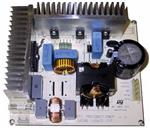
400 W FOT-controlled PFC pre-regulator with the L6563S
Introduction
This application note describes a demonstration board based on the transition-mode PFC
controller L6563S and presents the results of its bench evaluation. The board implements a
400 W, wide-range mains input, PFC pre-conditioner suitable for ATX PSU, flat screen
displays, etc. The chip is operated with fixed off time control in order to use a low-cost device
like the L6563S, which is usually prohibitive at this power level. Fixed-off-time control allows
continuous conduction mode operation, which is normally achieved with more expensive
control chips and more complex control architectures.
Figure 1.
November 2010
L6563S 400 W FOT PFC demonstration board (p/n EVL6563S-400W)
Doc ID 15796 Rev 2
1/38
www.st.com
�Contents
AN2994
Contents
1
Main characteristics and circuit description . . . . . . . . . . . . . . . . . . . . . 5
2
Test results and significant waveforms . . . . . . . . . . . . . . . . . . . . . . . . . 8
2.1
Harmonic content measurement . . . . . . . . . . . . . . . . . . . . . . . . . . . . . . . . 8
2.2
Inductor current in FOT and L6563S THD optimizer . . . . . . . . . . . . . . . . 12
2.3
Voltage feed-forward . . . . . . . . . . . . . . . . . . . . . . . . . . . . . . . . . . . . . . . . 14
2.4
Start-up and RUN pin . . . . . . . . . . . . . . . . . . . . . . . . . . . . . . . . . . . . . . . . 18
2.5
Brownout function . . . . . . . . . . . . . . . . . . . . . . . . . . . . . . . . . . . . . . . . . . . 19
2.6
Start-up at light loads . . . . . . . . . . . . . . . . . . . . . . . . . . . . . . . . . . . . . . . . 21
2.7
Overvoltage and open-loop protection . . . . . . . . . . . . . . . . . . . . . . . . . . . 22
2.8
Power management/housekeeping functions . . . . . . . . . . . . . . . . . . . . . . 24
3
Layout hints . . . . . . . . . . . . . . . . . . . . . . . . . . . . . . . . . . . . . . . . . . . . . . . 26
4
Audible noise . . . . . . . . . . . . . . . . . . . . . . . . . . . . . . . . . . . . . . . . . . . . . . 28
5
Thermal measures . . . . . . . . . . . . . . . . . . . . . . . . . . . . . . . . . . . . . . . . . . 29
6
Conducted emissions pre-compliance tests peak detection . . . . . . . 30
7
Bill of materials . . . . . . . . . . . . . . . . . . . . . . . . . . . . . . . . . . . . . . . . . . . . 31
8
PFC coil specification . . . . . . . . . . . . . . . . . . . . . . . . . . . . . . . . . . . . . . . 34
8.1
General description and characteristics . . . . . . . . . . . . . . . . . . . . . . . . . . 34
8.2
Electrical characteristics . . . . . . . . . . . . . . . . . . . . . . . . . . . . . . . . . . . . . . 34
8.3
Mechanical aspects and pin numbering . . . . . . . . . . . . . . . . . . . . . . . . . . 35
9
References . . . . . . . . . . . . . . . . . . . . . . . . . . . . . . . . . . . . . . . . . . . . . . . . 36
10
Revision history . . . . . . . . . . . . . . . . . . . . . . . . . . . . . . . . . . . . . . . . . . . 37
2/38
Doc ID 15796 Rev 2
�AN2994
List of figures
List of figures
Figure 1.
Figure 2.
Figure 3.
Figure 4.
Figure 5.
Figure 6.
Figure 7.
Figure 8.
Figure 9.
Figure 10.
Figure 11.
Figure 12.
Figure 13.
Figure 14.
Figure 15.
Figure 16.
Figure 17.
Figure 18.
Figure 19.
Figure 20.
Figure 21.
Figure 22.
Figure 23.
Figure 24.
Figure 25.
Figure 26.
Figure 27.
Figure 28.
Figure 29.
Figure 30.
Figure 31.
Figure 32.
Figure 33.
Figure 34.
Figure 35.
Figure 36.
Figure 37.
Figure 38.
Figure 39.
Figure 40.
Figure 41.
Figure 42.
Figure 43.
Figure 44.
Figure 45.
L6563S 400 W FOT PFC demonstration board (p/n EVL6563S-400W). . . . . . . . . . . . . . . . 1
EVL6563S-400W demonstration board: electrical schematic . . . . . . . . . . . . . . . . . . . . . . . 7
EVL6563S-400W compliance to EN61000-3-2 Standard at full load . . . . . . . . . . . . . . . . . . 8
EVL6563S-400W compliance to JEITA-MITI Standard at full load. . . . . . . . . . . . . . . . . . . . 8
EVL6563S-400W compliance to EN61000-3-2 Standard at 70 W load . . . . . . . . . . . . . . . . 8
EVL6563S-400W compliance to JEITA-MITI Standard at 70 W load . . . . . . . . . . . . . . . . . . 8
EVL6563S-400W input current waveform at 100 V, 60 Hz, 400 W load. . . . . . . . . . . . . . . . 9
EVL6563S-400W input current waveform at 230 V, 50 Hz, 400 W load. . . . . . . . . . . . . . . . 9
EVL6563S-400W input current waveform at 100 V, 60 Hz, 200 W load. . . . . . . . . . . . . . . . 9
EVL6563S-400W input current waveform at 230 V, 50 Hz, 200 W load. . . . . . . . . . . . . . . . 9
EVL6563S-400W input current waveform at 100 V, 60 Hz, 70 W load. . . . . . . . . . . . . . . . 10
EVL6563S-400W input current waveform at 230 V, 50 Hz, 70 W load. . . . . . . . . . . . . . . . 10
Power factor vs. Vin and load . . . . . . . . . . . . . . . . . . . . . . . . . . . . . . . . . . . . . . . . . . . . . . . 10
THD vs. Vin and load . . . . . . . . . . . . . . . . . . . . . . . . . . . . . . . . . . . . . . . . . . . . . . . . . . . . . 10
Efficiency vs. Vin and load . . . . . . . . . . . . . . . . . . . . . . . . . . . . . . . . . . . . . . . . . . . . . . . . . 11
Static Vout regulation vs. Vin and load . . . . . . . . . . . . . . . . . . . . . . . . . . . . . . . . . . . . . . . . 11
EVL6563S-400W inductor current ripple envelope at 115 Vac, 60 Hz, full load. . . . . . . . . 12
EVL6563S-400W inductor current ripple (detail) at 115 Vac, 60 Hz, full load . . . . . . . . . . 12
EVL6563S-400W inductor current ripple envelope at 230 Vac, 50 Hz, full load. . . . . . . . . 13
EVL6563S-400W inductor current ripple (detail) at 230 Vac, 50 Hz, full load . . . . . . . . . . 13
EVL6563S-400W input current shape at 100 Vac, 60 Hz, CFF = 470 nF, RFF = 390 kΩ . .15
EVL6563S-400W input current shape at 100 Vac, 60 Hz, CFF = 1.5 µF, RFF = 390 kΩ . .15
EVL6563S-400W input mains surge from 90 Vac to 140 Vac, full load, CFF = 1 µF . . . . . 16
L6562A FOT input mains surge from 90 Vac to 140 Vac, full load, NO VFF input . . . . . . . 16
EVL6563S-400W input mains dip from 140 to 90 Vac, full load, CFF = 1 µF. . . . . . . . . . . 17
L6562A FOT input mains dip from 140 to 90 Vac, full load, NO VFF input . . . . . . . . . . . . 17
EVL6563S-400W start-up at 90 Vac, 60 Hz, full load . . . . . . . . . . . . . . . . . . . . . . . . . . . . . 18
EVL6563S-400W start-up at 265 Vac, 50 Hz, full load . . . . . . . . . . . . . . . . . . . . . . . . . . . . 18
EVL6563S-400W start-up attempt at 80 Vac, 60 Hz, full load . . . . . . . . . . . . . . . . . . . . . . 19
EVL6563S-400W start-up with slow input voltage increase - full load . . . . . . . . . . . . . . . . 20
EVL6563S-400W turn-off with slow input voltage decrease - full load . . . . . . . . . . . . . . . . 20
EVL6563S-400W start-up at 265 V, 50 Hz, 30 mA load . . . . . . . . . . . . . . . . . . . . . . . . . . . 21
EVL6563S-400W start-up at 265 V, 50 Hz, no load and with external Vcc . . . . . . . . . . . . 21
EVL6563S-400W open loop at 115 Vac,60 Hz, full load . . . . . . . . . . . . . . . . . . . . . . . . . . 23
On/Off control by a cascaded converter controller via PFC_OK or RUN pin . . . . . . . . . . . 24
Interface circuits that let the L6563S switch a PWM controller on or off. . . . . . . . . . . . . . . 25
EVL6563S-400W PCB layout (not 1:1 scaled) . . . . . . . . . . . . . . . . . . . . . . . . . . . . . . . . . . 27
Thermal map at 115 Vac, 60 Hz - full load . . . . . . . . . . . . . . . . . . . . . . . . . . . . . . . . . . . . . 29
Thermal map at 230 Vac, 50 Hz - full load . . . . . . . . . . . . . . . . . . . . . . . . . . . . . . . . . . . . . 29
115 Vac and full load - phase . . . . . . . . . . . . . . . . . . . . . . . . . . . . . . . . . . . . . . . . . . . . . . . 30
115 Vac and full load - neutral . . . . . . . . . . . . . . . . . . . . . . . . . . . . . . . . . . . . . . . . . . . . . . 30
230 Vac and full load - phase . . . . . . . . . . . . . . . . . . . . . . . . . . . . . . . . . . . . . . . . . . . . . . . 30
230 Vac and full load - neutral . . . . . . . . . . . . . . . . . . . . . . . . . . . . . . . . . . . . . . . . . . . . . . 30
Electrical diagram . . . . . . . . . . . . . . . . . . . . . . . . . . . . . . . . . . . . . . . . . . . . . . . . . . . . . . . . 34
Side view of pin. . . . . . . . . . . . . . . . . . . . . . . . . . . . . . . . . . . . . . . . . . . . . . . . . . . . . . . . . . 35
Doc ID 15796 Rev 2
3/38
�List of tables
AN2994
List of tables
Table 1.
Table 2.
Table 3.
Table 4.
4/38
Measured temperature at 115 Vac and 230 Vac - full load . . . . . . . . . . . . . . . . . . . . . . . . 29
Bill of materials for the EVL6563S-400W demonstration board . . . . . . . . . . . . . . . . . . . . . 31
Winding characteristics . . . . . . . . . . . . . . . . . . . . . . . . . . . . . . . . . . . . . . . . . . . . . . . . . . . . 34
Document revision history . . . . . . . . . . . . . . . . . . . . . . . . . . . . . . . . . . . . . . . . . . . . . . . . . 37
Doc ID 15796 Rev 2
�AN2994
1
Main characteristics and circuit description
Main characteristics and circuit description
The EVL6563S-400W demonstration board has the following characteristics.
●
Line voltage range: 90 to 265 Vac
●
Minimum line frequency (fL): 47 Hz
●
Regulated output voltage: 400 V
●
Rated output power: 400 W
●
Maximum 2fL output voltage ripple: 10 V pk-pk
●
Hold-up time: 22 ms (VDROP after hold-up time: 300 V)
●
Maximum switching frequency: 85 kHz (Vin = 90 Vac, Pout = 400 W)
●
Minimum estimated efficiency: 90% (Vin = 90 Vac, Pout = 400 W)
●
Maximum ambient temperature: 50 °C
●
EMI: in accordance with EN55022 Class-B
●
PCB type and size: single side, 70 µm, CEM-1, 148.5 x 132 mm
●
Low profile design: 35 mm component maximum height
The demonstration board implements a power factor correction (PFC) pre-regulator
delivering 400 W of continuous power on a regulated 400 V rail from a wide-range mains
voltage, and providing for the reduction of the mains harmonics, thus complying with the
European norm EN61000-3-2 and the Japanese norm JEITA-MITI. This rail will be the input
for the cascaded isolated DC-DC converter that will provide the output voltages required by
the load.
The board is equipped with enough heat sinking to allow full-load operation in still air. With
an appropriate airflow and without any change in the circuit, the demonstration board can
easily deliver up to 450 W.
The controller is the L6563S (U1), integrating all the functions needed to control the PFC
stage and to interface with the downstream converter. The L6563S controller chip is
designed for transition-mode (TM) operation, where the boost inductor works next to the
boundary between continuous (CCM) and discontinuous conduction mode (DCM). However,
with a slightly different usage, the chip can operate so that the boost inductor works in CCM,
hence surpassing the limitations of TM operation in terms of power handling capability. The
gate-drive capability of the L6563S is also adequate to drive the MOSFETs used at higher
power levels. This approach, which couples the simplicity and cost-effectiveness of TM
operation with the high-current capability of CCM operation, is the fixed off time (FOT)
control. The control modulates the ON time of the power switch, while its OFF time is kept
constant. More precisely, the line-modulated FOT (LM FOT) is used, where the OFF time of
the power switch is not rigorously constant but is modulated by the instantaneous mains
voltage. Refer to [2] for a detailed description of this technique.
The power stage of the PFC is a conventional boost converter, connected to the output of
the rectifier bridge D2. It includes the coil L4, the diode D3 and the capacitors C6 and C7.
The boost switch is represented by the power MOSFETs Q1 and Q2. The NTC R2 limits the
inrush current at switch on. It has been connected to the DC rail, in series to the output
electrolytic capacitor, in order to improve the efficiency during low line operation.
Additionally, the splitting into two of the output capacitors (C6 and C7) means that the AC
current is mainly managed by the film capacitor C7, making the electrolytic cheaper
because it only has to bear the DC part.
Doc ID 15796 Rev 2
5/38
�Main characteristics and circuit description
AN2994
At start-up the L6563S is powered by the Vcc capacitor (C12) that is charged via the
resistors R3 and R4, and then the L4 secondary winding (pins 8-11), and the charge pump
circuit (R5, C10, D5 and D4) generates the Vcc voltage that powers the L6563S during
normal operations.
The dividers R32, R33 and R34 provide the L6563S multiplier with information relating to
the instantaneous voltage used to modulate the boost current. The same information is also
used to obtain the average value of the AC line by the voltage feed-forward (VFF) pin. The
dividers R9, R10, R11, R12 and 13 are dedicated to sensing the output voltage while the
dividers R6, R7, R8 and R24 are dedicated to protecting the circuit in case of voltage loop
failures. The line-modulated FOT is obtained by the timing generator components D6, C15,
R15, C16, R16, R31, Q3.
The board is equipped with an input EMI filter designed for a two-wire input mains plug. It is
composed of two stages: a common-mode pi-filter connected at the input (C1, L1, C2, C3)
and a differential-mode pi-filter after the input bridge (C4, L3, C5). It also offers the
possibility of easily connecting a downstream converter and testing the interface signals
managed by the L6563S.
6/38
Doc ID 15796 Rev 2
����� ���9DF
�
�
Doc ID 15796 Rev 2
5��
��� N
��� N
&��
�X)
�0�
5�
5��
5��
��.
�0�
5�
�0�
5�
�0�
5�
���� 9GF
�$���� 9
&��
��Q )
�
�
��
��
��
&��
��Q )
�0�
3:0�/$7&+
��
��
�X)
��N
5��
58 1
=&'
*1'
*'
9&&
��N
5��
��� N
5��
�5�
5���
3:0�6723
8�
/���� 6
3)&�2.
7%2
9))
&6
08/7
&203
,19
��.
5��
�
5��
�
�
�
�
�
�
�
- 3���
- 803(5
��� N
5��
�
���Q )�;�
&�
/�
5(6
�
&��
��� N
5�
��N
/�
5��
5��
��N
&��
���Q )
���Q )�;�
&�
&0����P+��$
- 3���
- 803(5
&�
5(6
�Q)�
&��
&�
5(6
���Q )�;�
&�
5��
5(6
5��
5(6
5(6
�
�
�
-�
&��
���S )
���Q )���� 9
5��
��.
&��
���S )
/�
'0���X +��$
&�
4�
%&��� &
5��
�N�
��X )���9
5��
5(6
&��
���Q )���9
�
�
&��
a
a
'�
'��;%��
5��
�.�
5���
�5�
//��� �
'�
���Q )���� 9
&�
'�
//��� �
5�
��� .
5�
��� .
�
���S )
&��
5��
�5�
5��
�5�
5��
�5�
5��
�5�
'�
%=;���&��
&��
��1
5�
��5
���
�.�
5��
��
/�
34������X +
���
'�
//��� �
'�
//��� �
5��
5��
�5����: �5����:
���� 9GF
5��
�5����:
5��
�5����:
4�
673��10��)3
&�
���X )���� 9
17&��5��6���
5�
���Q )���� 9
&�
4�
673��10��)3
677+�5��
'�
�1��� �
'�
-�
����9GF
����9GF
1&
571
571
����9RX W
�
�
�
�
�
Figure 2.
-�
)�
�
AN2994
Main characteristics and circuit description
EVL6563S-400W demonstration board: electrical schematic
".�����W�
7/38
�Test results and significant waveforms
AN2994
2
Test results and significant waveforms
2.1
Harmonic content measurement
One of the main purposes of a PFC pre-conditioner is to correct the input current distortion,
decreasing the harmonic contents below the limits of the relevant regulations. Therefore, the
board has been tested according to the European rule EN61000-3-2 Class-D and Japanese
rule JEITA-MITI Class-D, at full load and 70 W output power, at both the nominal input
voltage mains.
As shown in the following figures, the circuit can reduce the harmonics well below the limits
of both regulations from full load down to light load. An output power of 70 W has been
chosen because it is almost the lower power limit at which the harmonics have to be limited
according the mentioned rules.
Figure 3.
EVL6563S-400W compliance to
EN61000-3-2 Standard at full load
Measured value
EN61000-3-2 Class-D limits
Figure 4.
Measur ed value
Har monic Current [A]
Har monic Current [A]
JEIT A-MITI limits
10
10
1
0.1
0.01
0.001
0.0001
1
0.1
0.01
0.001
0.0001
1 3 5 7 9 11 13 15 17 19 21 23 25 27 29 31 33 35 37 39
1 3 5 7 9 11 13 15 17 19 21 23 25 27 29 31 33 35 37 39
Harmonic Ord er [n]
Harmon ic Or der [n]
Figure 5.
EVL6563S-400W compliance to
JEITA-MITI Standard at full load
EVL6563S-400W compliance to
Figure 6.
EN61000-3-2 Standard at 70 W load
Measured value
EN61000-3-2 Class-D limits
EVL6563S-400W compliance to
JEITA-MITI Standard at 70 W load
Measured value
JEITA-MITI limits
1
Harmon ic Cu rrent [A]
Harmonic Curr ent [A]
1
0.1
0.01
0.001
0.1
0.01
0.001
0.0001
0.0001
1 3 5 7 9 11 13 15 17 19 21 23 25 27 29 31 33 35 37 39
Harmonic Order [n]
8/38
Doc ID 15796 Rev 2
1 3 5 7 9 11 13 15 17 19 21 23 25 27 29 31 33 35 37 39
H armo nic O rder [n]
�AN2994
Test results and significant waveforms
For reference, the following waveforms show the input current and voltage at the nominal
input voltage mains and at different load conditions.
Figure 7.
EVL6563S-400W input current
waveform at 100 V, 60 Hz, 400 W
load
Figure 8.
EVL6563S-400W input current
waveform at 230 V, 50 Hz, 400 W
load
CH1: Rectified mains voltage
CH4: Input current
CH1: Rectified mains voltage
CH4: Input current
Figure 9.
Figure 10. EVL6563S-400W input current
waveform at 230 V, 50 Hz, 200 W
load
EVL6563S-400W input current
waveform at 100 V, 60 Hz, 200 W
load
CH1: Rectified mains voltage
CH4: Input current
CH1: Rectified mains voltage
CH4: Input current
Doc ID 15796 Rev 2
9/38
�Test results and significant waveforms
AN2994
Figure 11. EVL6563S-400W input current
Figure 12. EVL6563S-400W input current
waveform at 100 V, 60 Hz, 70 W load
waveform at 230 V, 50 Hz, 70 W load
CH1: Rectified mains voltage
CH4: Input current
CH1: Rectified mains voltage
CH4: Input current
The power factor (PF) and the total harmonic distortion (THD) have also been measured
and the results are reported in Figure 13 and Figure 14. As shown, the PF at full load and
half load remains close to unity throughout the input voltage mains range, while when the
circuit is delivering 70 W it decreases at a high mains range. THD is low, remaining within
20% at the maximum input voltage.
Figure 13. Power factor vs. Vin and load
Figure 14. THD vs. Vin and load
THD[% ]
25
PF
1
0.95
20
0.9
15
400W
200W
400W
0.85
70W
10
200W
70W
0.8
5
0
0.75
90
100
115
130
Vin [Vrms]
180
230
265
90
100
115
130
Vin [Vrms ]
180
230
265
The converter’s efficiency reported in Figure 15 is very good at all load and line conditions.
At full load, it is always significantly higher than 90%, making this design suitable for highefficiency power supplies.
The measured output voltage variation at different line and load conditions is reported in
Figure 16. As shown, thanks to the voltage feed-forward function embedded in the L6563S,
the voltage is perfectly stable over the entire input voltage range. At 265 Vac and light load,
there is a negligible deviation of 1 V due to the intervention of the burst mode function.
10/38
Doc ID 15796 Rev 2
�AN2994
Test results and significant waveforms
Figure 15. Efficiency vs. Vin and load
Figure 16. Static Vout regulation vs. Vin and
load
Eff. [%]
98%
Vout [Vdc ]
408.0
400 W
96%
407.5
93%
407.0
91%
406.5
200 W
70W
400W
88%
15W
406.0
200W
405.5
70W
86%
405.0
83%
90
100
115
130
180
230
265
90
Vin [Vrms]
Doc ID 15796 Rev 2
100
115
130
Vin [Vrms]
180
230
265
11/38
�Test results and significant waveforms
2.2
AN2994
Inductor current in FOT and L6563S THD optimizer
The following figures show the waveforms of the inductor current at different voltage mains:
as shown in Figure 17 and Figure 19, the inductor current waveform over the half-period of a
line is very similar to that of a CCM PFC. Figure 18 and Figure 20 (magnifications of the
waveforms at the peak of the sine wave), show the different ripple currents and OFF times,
which are modulated by the input mains voltage. It is also possible to note the transition
angle from DCM to CCM, which occurs closer to the zero crossing of the current sine wave
at low mains and moves towards the top if the circuit is working at high mains.
Figure 17. EVL6563S-400W inductor current
ripple envelope at 115 Vac, 60 Hz,
full load
Figure 18. EVL6563S-400W inductor current
ripple (detail) at 115 Vac, 60 Hz,
full load
CH1: Q1/Q2 drain voltage
CH2: MULT voltage - pin #3
CH4: L4 inductor current ripple envelope
CH1: Q1/Q2 drain voltage
CH2: MULT voltage - pin #3
CH4: L4 inductor current ripple envelope
12/38
Doc ID 15796 Rev 2
�AN2994
Test results and significant waveforms
On both the drain voltage traces reported in Figure 18 and Figure 20, close to the zero
crossing points of the sine wave it is possible to note the action of the THD optimizer
embedded in the L6563S. This optimizer is a circuit that minimizes the conduction’s deadangle occurring at the AC’s input current near the zero-crossings of the line voltage
(crossover distortion). In this way, the THD of the current is considerably reduced. A major
cause of this distortion is the inability of the system to transfer energy effectively when the
instantaneous line voltage is very low. This effect is magnified by the high-frequency filter
capacitor placed after the bridge rectifier, which retains some residual voltage that causes
the diodes of the bridge rectifier to be reverse-biased and the input current flow to
temporarily stop. To overcome this issue, the device forces the PFC pre-regulator to process
more energy near the line voltage’s zero-crossing, as compared to that commanded by the
control loop.
This results in minimizing the time interval where energy transfer is lacking and fully
discharging the high-frequency filter capacitor after the bridge. Essentially, the circuit
artificially increases the ON time of the power switch with a positive offset added to the
output of the multiplier in the proximity of the line voltage zero crossing. This offset is
reduced as the instantaneous line voltage increases, so that it becomes negligible as the
line voltage moves towards the top of the sinusoid, and it is modulated by the voltage on the
VFF pin so as to have little offset at low lines, where the transfer of energy at zero crossings
is typically quite good, and a larger offset at high lines, where the energy transfer gets
worse.
To get the maximum benefit from the THD optimizer circuit, the high-frequency filter
capacitors after the bridge rectifier should be minimized, compatibly with EMI filtering needs.
A large capacitance, in fact, introduces a conduction dead-angle of the AC input current in
itself, thus reducing the effectiveness of the optimizer circuit.
Figure 19. EVL6563S-400W inductor current
ripple envelope at 230 Vac, 50 Hz,
full load
Figure 20. EVL6563S-400W inductor current
ripple (detail) at 230 Vac, 50 Hz,
full load
CH1: Q1/Q2 drain voltage
CH2: MULT voltage - pin #3
CH4: L4 inductor current ripple envelope
CH1: Q1/Q2 drain voltage
CH2: MULT voltage - pin #3
CH4: L4 inductor current ripple envelope
Doc ID 15796 Rev 2
13/38
�Test results and significant waveforms
2.3
AN2994
Voltage feed-forward
The power stage gain of PFC pre-regulators varies with the square of the RMS input
voltage. So does the crossover frequency (fc) of the overall open-loop gain because the gain
has a single pole characteristic. This leads to large trade-offs in the design. For example,
setting the gain of the error amplifier to get an fc of 20 Hz at 264 Vac means having an fc of
4 Hz at 88 Vac, resulting in sluggish control dynamics. Additionally, the slow control loop
causes large transient current flows during rapid line or load changes that are limited by the
dynamics of the multiplier output. This limit is considered when selecting the sense resistor
to let the full load power pass under minimum line voltage conditions, with some margin. But
a fixed current limit allows excessive power inputs at high lines, whereas a fixed power limit
requires the current limit to vary inversely with the line voltage.
The voltage feed-forward function can compensate for the gain variation with the line voltage
and allow overcoming all of the above-mentioned issues. It consists of deriving a voltage
proportional to the input RMS voltage, feeding this voltage into a squarer/divider circuit
(1/V2 corrector) and providing the resulting signal to the multiplier that generates the current
reference for the inner current-control loop. In this way, a change of the line voltage will
cause an inversely proportional change of the half sine amplitude at the output of the
multiplier so that the current reference is adapted to the new operating conditions with
(ideally) no need for invoking the slow dynamics of the error amplifier. Additionally, the loop
gain will be constant throughout the input voltage range, which significantly improves
dynamic behavior at low lines and simplifies loop design.
The L6563S realizes a voltage feed-forward with a technique that makes use of just two
external parts and that limits the feed-forward time constant trade-off issue to only one
direction. A capacitor CFF (C18) and a resistor RFF (R26 + R27), both connected to the VFF
pin (5), complete an internal peak-holding circuit that provides a DC voltage equal to the
peak of the rectified sine wave applied on the MULT pin (pin 3). RFF provides a means of
discharging CFF when the line voltage decreases.
However, a drawback of the VFF technique is an increase in the harmonics; in fact, deriving
a voltage proportional to the RMS line voltage implies a form of integration, which has its
own time constant. If it is too small, the voltage generated will be affected by a considerable
amount of ripple at twice the mains frequency, thus causing a distortion of the current
reference (resulting in high THD and poor PF). If it is too large, there will be a considerable
delay in setting the right amount of feed forward, resulting in excessive overshoot and
undershoot of the pre-regulator's output voltage in response to large line voltage changes.
Clearly, a trade-off is required. For reference, Figure 21 and Figure 22 show a comparison
of the input current shape and the measurement of the THD and 3RD harmonic amplitude
for different CFF values taken from a similar board using the former L6563.
14/38
Doc ID 15796 Rev 2
�AN2994
Test results and significant waveforms
Figure 21. EVL6563S-400W input current
shape at 100 Vac, 60 Hz,
CFF = 470 nF, RFF = 390 kΩ
Figure 22. EVL6563S-400W input current
shape at 100 Vac, 60 Hz,
CFF = 1.5 µF, RFF = 390 kΩ
THD [%]: 3.39% - 3RD harmonic: 0.126 A
CH3: VFF voltage - pin #5
CH4: Input current
THD [%]: 2.75% - 3RD harmonic: 0.109 A
CH3: VFF voltage - pin #5
CH4: Input current
To overcome this issue, the new L6563S integrates an innovative circuitry that allows getting
a fast transient response regardless of the voltage change that occurs on the mains, both
surges and drops. Therefore, if there is a sudden rise in the line voltage, CFF is rapidly
charged through the low impedance of the internal diode and no appreciable overshoot is
visible at the pre-regulator's output. If there is a drop in the line voltage, an internal "mains
drop" detector enables a low impedance switch that suddenly discharges CFF, therefore
avoiding a long settling time before reaching the new voltage level. Consequently, an
acceptably low steady-state ripple and low current distortion can be achieved without any
considerable undershoot or overshoot on the pre-regulator's output like in systems with no
feed-forward compensation.
Figure 23 shows the behavior of the EVL6563S-400W demonstration board in the case of
an input voltage surge from 90 to 140 Vac: in the graphic, it is evident that the VFF function
provides for the stability of the output voltage, which is not affected by the input voltage
surge. In fact, thanks to the VFF function, the compensation of the input voltage variation is
very fast and the output voltage remains stable at its nominal value. The opposite is
confirmed in Figure 24: it shows the behavior of a PFC using the L6562 operating in FOT
and delivering a similar output power. In the case of a mains surge, the controller cannot
compensate it and the output voltage stability is guaranteed by the feedback loop only.
Unfortunately, as previously said, its bandwidth is narrow and thus the output voltage has a
significant deviation from the nominal value. The circuit has the same behavior in the case of
a mains surge at any input voltage, and is also not affected if the input mains surge happens
at any point of the input sine wave.
Doc ID 15796 Rev 2
15/38
�Test results and significant waveforms
AN2994
Figure 23. EVL6563S-400W input mains surge Figure 24. L6562A FOT input mains surge
from 90 Vac to 140 Vac, full load,
from 90 Vac to 140 Vac, full load,
CFF = 1 µF
NO VFF input
CH1: Output voltage
CH2: Input rectified mains voltage
CH3: VFF voltage - pin #5
CH4: Input current
CH1: Output voltage
CH2: Input rectified mains voltage
CH4: Input current
Figure 25 shows the circuit’s behavior in the case of a mains dip: as previously described,
the internal circuitry has detected the decreasing of the mains voltage and has activated the
CFF internal fast discharge. As you can see in this case, the output voltage changes but
within a few mains cycles it comes back to the nominal value. The situation is different if we
check the performance of a controller without the VFF function. Figure 26 shows the
behavior of a PFC using the L6562A operating in FOT and delivering a similar output power:
in the case of a mains dip from 140 to 90 Vac, the output voltage variation is not very
different but the output voltage requires a longer time to restore the original value.
Doing tests with a wider voltage variation (for example, 265 to 90 Vac) the output voltage
variation of a PFC without the voltage feed-forward fast discharge is much more
emphasized.
16/38
Doc ID 15796 Rev 2
�AN2994
Test results and significant waveforms
Figure 25. EVL6563S-400W input mains dip
from 140 to 90 Vac, full load,
CFF = 1 µF
Figure 26. L6562A FOT input mains dip from
140 to 90 Vac, full load,
NO VFF input
CH1: Output voltage
CH2: Input rectified mains voltage
CH3: VFF voltage - pin #5
CH4: Input current
CH1: Output voltage
CH2: Input rectified mains voltage
CH4: Input current
If you compare Figure 21 and Figure 22 to Figure 23 and Figure 25, you can see that the
input current of the last two figures is much better and the 3rd harmonic current distortion is
not noticeable. This demonstrates the benefits of the new voltage feed-forward circuit
integrated in the L6563S, allowing you to get a fast response to mains disturbances and a
very low THD and high PF at the same time.
Doc ID 15796 Rev 2
17/38
�Test results and significant waveforms
2.4
AN2994
Start-up and RUN pin
Figure 27 and Figure 28 show the waveforms during the start-up of the circuit, at mains
plug-in. The Vcc voltage rises up to the turn-on threshold, and the L6563S starts the
operation. For a short time the energy is supplied by the Vcc capacitor, then the auxiliary
winding and the charge pump circuit take over. At the same time, the output voltage rises
from the peak value of the rectified mains to the nominal value of the PFC output voltage.
The good phase margin of the compensation network allows a clean start-up, without any
large overshoot.
Figure 27. EVL6563S-400W start-up
at 90 Vac, 60 Hz, full load
Figure 28. EVL6563S-400W start-up
at 265 Vac, 50 Hz, full load
CH1: Output voltage
CH2: Pin #14 - Vcc voltage
CH3: Pin #10 - RUN
CH4: Pin #13 - Gate drive
CH1: Output voltage
CH2: Pin #14 - Vcc voltage
CH3: Pin #10 - RUN
CH4: Pin #13 - Gate drive
18/38
Doc ID 15796 Rev 2
�AN2994
2.5
Test results and significant waveforms
Brownout function
A dangerous event for any PFC is the operation during a mains undervoltage. This condition
may cause overheating of the power section due to an excess of RMS current. To protect
the PFC from this abnormal operation, a brownout protection is needed. It is basically a nonlatched shutdown function that has to be activated when a mains undervoltage condition is
detected.
The L6563S has a dedicated inhibit pin (RUN, #10) that embeds a comparator with
hysteresis and which stops the L6563S operation if the voltage applied is below its
threshold. Because the L6563S VFF pin delivers a voltage signal proportional to the input
mains, the complete brownout function can be easily realized using a simple resistor divider
connected between the VFF and RUN pins. In this demonstration board, the divider resistors
setting the turn-on threshold are R26 and R27 on the schematic in Figure 1. Figure 29
shows a start-up tentative below the threshold. As visible at start-up, the RUN pin does not
allow the PFC start-up.
Figure 29. EVL6563S-400W start-up attempt at 80 Vac, 60 Hz, full load
CH1: Output voltage
CH2: Pin #14 - Vcc voltage
CH3: Pin #10 - RUN
CH4: Pin #13 - Gate drive
Figure 30 and Figure 31 show the waveforms of the circuit during operation of the brownout
protection. In both cases, the mains voltages were increased or decreased slowly. As you
can see, at both turn-on and turn-off, there are no bouncing or starting attempts by the
converter.
Doc ID 15796 Rev 2
19/38
�Test results and significant waveforms
AN2994
Figure 30. EVL6563S-400W start-up with slow Figure 31. EVL6563S-400W turn-off with slow
input voltage increase - full load
input voltage decrease - full load
CH1: Output voltage
CH2: Pin #14 - Vcc voltage
CH3: Pin #10 - RUN
CH4: Pin #13 - gate drive
20/38
CH1: Output voltage
CH2: Pin #14 - Vcc voltage
CH3: Pin #10 - RUN
CH4: Pin #13 - gate drive
Doc ID 15796 Rev 2
�AN2994
2.6
Test results and significant waveforms
Start-up at light loads
Figure 32. EVL6563S-400W start-up
at 265 V, 50 Hz, 30 mA load
Figure 33. EVL6563S-400W start-up at 265 V,
50 Hz, no load and with external
Vcc
CH1: Q1/Q2 drain voltage
CH2: Output voltage
CH3: Pin #13 - gate drive
CH4: Pin #14 - Vcc voltage
CH1: Q1/Q2 drain voltage
CH2: Output voltage
CH3: Pin #13 - gate drive
CH4: Pin #14 - Vcc voltage
The board, as it is, is able to properly handle an output load as low as 12 W. With lower load
levels, the system will not start up correctly at high lines because burst pulses last so long
that the Vcc voltage drops below the UVLO of the L6563S. In such conditions, if the load
increases suddenly, the PFC output voltage will drop until the IC resumes normal operation.
When the L6563S is supplied from an external source (typically, it is the auxiliary voltage
that powers the controller of the downstream converter or an auxiliary power supply), the
minimum load that can be handled properly goes to virtually zero. The start-up behavior at
the minimum load (12 W) is reported in Figure 32. It can be noted that the self-supply circuit
connected to the auxiliary winding of the inductor is working properly.
Figure 33 shows the circuit start-up at no load, with the L6563S powered by an external Vcc
(15 V). The PFC regulates the output voltage perfectly.
Doc ID 15796 Rev 2
21/38
�Test results and significant waveforms
2.7
AN2994
Overvoltage and open-loop protection
Normally, the voltage-control loop keeps the output voltage Vo of the PFC pre-regulator
close to its nominal value, set by the ratio of the resistors of the output divider (R9, R10, R11
and R12 in parallel to R13). The device’s PFC_OK pin (#7) is dedicated to monitoring the
output voltage with a separate resistor divider (R6, R7, R8 and R24). This divider has been
selected so that the voltage at the pin reaches 2.5 V if the output voltage exceeds a preset
value, usually higher than the maximum Vo that can be expected, also including worst-case
load/line transients.
When this function is triggered, the activity of the gate drive is immediately stopped until the
voltage on the PFC_OK pin drops below 2.4 V. Notice that R1, R2, R3 and R4 can be
selected without any constraints.
The unique criterion is that both dividers have to sink a current from the output bus, which
needs to be significantly higher than the current biasing the error amplifier and PFC_OK
comparator.
The OVP function described above can handle “normal” overvoltage conditions, that is,
those resulting from an abrupt load/line change or occurring at start-up. If the overvoltage is
generated by a feedback disconnection, for instance, when the upper resistor of the output
divider fails to open, an additional circuitry detects the voltage drop of the INV pin. If the
voltage on pin INV is lower than 1.66 V and at the same time the OVP is active, the feedback
failure is assumed. Hence, the gate drive activity is immediately stopped, the device is shut
down, its quiescent consumption is reduced to below 180 μA and the condition is latched as
long as the supply voltage of the IC stays above the UVLO threshold. At the same time, the
PWM_LATCH pin is asserted high. PWM_LATCH is an open-source output that can deliver
2.8 V minimum with a 0.25 mA load, intended for tripping a latched shutdown function of the
PWM controller IC in the cascaded DC-DC converter, so that the entire unit is latched off. In
this case, to resume operation, it is necessary to recycle the input power so that the Vcc
voltage of the L6563S goes below 6 V and that one of the PWM controller goes below its
UVLO threshold.
The PFC_OK pin doubles its function as a non-latched IC disable: a voltage below 0.23 V
will shut down the IC, reducing its consumption to below 2 mA. In this case, both
PWM_STOP and PWM_LATCH keep their high impedance status. To restart the IC, simply
let the voltage at the pin go above 0.27 V.
Note that this function offers a complete protection against not only feedback loop failures or
erroneous settings, but also against a failure of the protection itself. Either resistor of the
PFC_OK divider failing short or open or a PFC_OK pin floating will result in the IC being
shut down and the pre-regulator stopped.
The event of an open loop is captured in Figure 34, where you can see the protection
intervention stopping the operation of the L6563S and the activation of the PWM_LATCH
pin.
22/38
Doc ID 15796 Rev 2
�AN2994
Test results and significant waveforms
Figure 34. EVL6563S-400W open loop at 115 Vac,60 Hz, full load
CH1: Q1/Q2 drain voltage
CH2: Output voltage
CH3: Pin #7 - PFC_OK
CH4: Pin #8 - PWM_LATCH
Doc ID 15796 Rev 2
23/38
�Test results and significant waveforms
2.8
AN2994
Power management/housekeeping functions
A special feature of the L6563S is that it facilitates the implementation of the "housekeeping"
circuitry needed to coordinate the operation of the PFC stage with that of the cascaded DCDC converter. The functions realized by the housekeeping circuitry ensure that transient
conditions such as power-up or power-down sequencing or failures of either power stage
are properly handled. The L6563S provides some pins for this purpose.
As already mentioned, one communication line between the L6563S and the PWM
controller of the cascaded DC-DC converter is the PWM_LATCH pin (#8), which is normally
open when the PFC works properly. It goes high if the L6563S loses control of the output
voltage (because of a failure of the control loop) or if the boost inductor saturates, with the
aim of latching off the PWM controller of the cascaded DC-DC converter as well.
A second communication line can be established via the disable function included in the
RUN pin. Typically, this line is used to allow the PWM controller of the cascaded DC-DC
converter to shut down the L6563S in the case of a light load to minimize the no-load input
consumption of the power supply.
Figure 35. On/Off control by a cascaded converter controller via PFC_OK or RUN pin
���K7
62%&
,����
OR
,����!
��
0&#?34/0
0&#?/+
�
�25.
���
0&#?/+
�
�25.
,����3
,����
�
,����3
���
���K7
"#���
�� 0&#?34/0
��
6##?0&#
,����!
6##
��
,����3
!-�����V�
The third communication line is the PWM_STOP pin (pin #9), which works in conjunction
with the RUN pin (pin #10). The purpose of the PWM_STOP pin is to inhibit the PWM
activity of both the PFC stage and the cascaded DC-DC converter. The pin is an open
collector, normally open, that goes low if the device is disabled by a voltage lower than 0.8 V
on the RUN pin (#10). It is important to point out that this function works correctly in systems
where the PFC stage is the master and the cascaded DC-DC converter is the slave or, in
other words, where the PFC stage starts first, powers both controllers and enables/disables
the operation of the DC-DC stage. This function is quite flexible and can be used in different
ways. In systems comprising an auxiliary converter and a main converter (for example, a
desktop PC's silver box or Hi-end flat-TV or monitor), where the auxiliary converter also
powers the controllers of the main converter, the RUN pin (#10) can be used to start and
stop the main converter. In the simplest case, to enable/disable the PWM controller, the
PWM_STOP (#9) pin can be connected to either the output of the error amplifier or, if the
chip is provided with it, to its soft-start pin.
The EVL6563S-400W offers the possibility to test these functions by connecting it to the
cascaded converter via the series resistors R28, R29, R30 and the connector J3. If the
PWM_STOP (#9) pin, which is an open-collector type, needs a pull-up resistor, connect it
close to the cascaded PWM for better noise immunity.
24/38
Doc ID 15796 Rev 2
�AN2994
Test results and significant waveforms
Figure 36. Interface circuits that let the L6563S switch a PWM controller on or off
��
�
/.
25.
���
���
/&&
,�����!�8��OR��
�
5#���X�8���
�
5#���X�8���
�
,������ 8��OR��
�
�
� �
,�����8��OR��
,����!�8��OR� � �
,����!�"�8���
�
��
��
�
� � �� � 07-?34/0���
,����3�
07-�2%3��
CONTROLLER���
8
��
�
07-�2%3��
CONTROLLER���
8
� � 07-?,!4#(��
��
,�����!�8����
�
,�����8���
,����!�8��
� ��
,����!�"�8��
�
D��QRW�ODWFKHG���
�
,����3�
��
E��ODWFKHG���
��
!-�����V�
Doc ID 15796 Rev 2
25/38
�Layout hints
3
AN2994
Layout hints
The layout of any converter is a very important phase in the design process that sometimes
does not get the required attention by engineers. Even if the layout phase is sometimes
time-consuming, a good layout saves time during the functional debugging and qualification
phases. Additionally, a power supply circuit with a correct layout needs smaller EMI filters or
less filter stages and therefore contributes to money saving.
The L6563S does not require any specific attention to the layout. General layout rules for
any power converter have to be applied carefully. These basic rules are listed below, taking
the EVL6563S-400W schematic as reference. They can be used for other PFC circuits with
any power level, working either in FOT or TM control mode.
26/38
1.
Keep the power and signal RTN separate. Connect the return pins of the component
carrying the high current, such as the C4, C5 input filter, sense resistors, C6 and C7
output capacitor, as close as possible. This point will be the RTN’s start point. A
downstream converter will have to be connected to this return point.
2.
Minimize the length of the traces relevant to L3, boost inductor L4, MOSFET drain,
boost rectifier D4 and output capacitors C6 and C7.
3.
Keep signal components as close as possible to each relevant pin of the L6563S. Keep
the tracks relevant to pin #1 (INV) as short as possible. Components and traces
relevant to the error amplifier have to be placed far from traces and connections
carrying signals with high dv/dt like the MOSFET drains (Q1 and Q2).
4.
Connect heat sinks to the power GND.
5.
Add an external shield to the boost inductor and connect it to the power GND.
6.
Connect the RTN of the signal components, including the feedback, PFC_OK and
MULT dividers, close to the L6563S’ pin #12 (GND).
7.
Connect a ceramic capacitor (100÷470 nF) to pin #14 (Vcc) and to pin #12 (GND),
close to the L6563S. Connect this point to the RTN’s start point (see 1).
Doc ID 15796 Rev 2
�AN2994
Layout hints
Figure 37. EVL6563S-400W PCB layout (not 1:1 scaled)
Doc ID 15796 Rev 2
27/38
�Audible noise
4
AN2994
Audible noise
Differential mode currents in a circuit with high- and low-frequency components (like in a
PFC) may produce audible noise due to inter-modulation between the operating frequency
and the mains line frequency.
This phenomenon occurs because of the mechanical vibration of reactive components like
capacitors and inductors. Current flowing in the winding can cause the vibration of wires or
ferrite, and as such produce buzzing noise. To avoid this, the boost and filter inductors have
to be wound with a correct wire tension and the component has to be varnished or dipped.
Frequently, X-capacitors and filter capacitors after the bridge generate acoustic noise
because of AC current that causes the electrodes to vibrate, producing buzzing noise. Thus,
minimizing the AC current by inserting a differential-mode, Pi filter between the bridge and
the boost inductor helps to reduce the acoustic noise. The EMI filter will also benefit from
this. In fact, such a filter significantly decreases the ripple current that otherwise has to be
filtered by the EMI filter. The capacitors to be selected are of a polypropylene (preferably
dipped) type because boxed ones are generally more at risk of generating acoustic noise.
28/38
Doc ID 15796 Rev 2
�AN2994
5
Thermal measures
Thermal measures
To verify the reliability of the design, a thermal mapping by means of an IR camera has been
done. Figure 38 and Figure 39 show the thermal measurements on the board component
side at nominal input voltages and full load. Pointers (visible on the images) placed across
the key components show the relevant temperature. Table 1 provides the correlation
between the measured points and the components, for both thermal maps. The ambient
temperature during both measurements was 27°C. According to the results obtained, all the
board components are operating within their temperature limits.
Figure 38. Thermal map at 115 Vac, 60 Hz - full load
Figure 39. Thermal map at 230 Vac, 50 Hz - full load
Table 1.
Measured temperature at 115 Vac and 230 Vac - full load
Point
Component
Temperature at 115 Vac
Temperature at 230 Vac
A
D2
57.3 °C
42.3 °C
B
Q2
62.2 °C
48.6 °C
C
Q1
62.4 °C
48.3 °C
D
D3
60.2 °C
47.8 °C
E
C7
38.2 °C
35.4 °C
F
L1
53.4 °C
37.2 °C
G
L3
55.1 °C
40.1 °C
H
L4 – CORE
61.8 °C
49.3 °C
I
L4 – WINDING
68.7 °C
52.8 °C
Doc ID 15796 Rev 2
29/38
�Conducted emissions pre-compliance tests peak detection
6
AN2994
Conducted emissions pre-compliance tests peak
detection
The following figures show the peak measurement of the conducted noise at full load and
nominal mains voltages. The limits shown on the diagrams are relevant to the EN55022
Class-B, the most popular norm for domestic equipment using a two-wire mains connection.
As shown, a good margin of the measures with respect to the limits is achieved in all test
conditions.
Figure 40. 115 Vac and full load - phase
Figure 41. 115 Vac and full load - neutral
Figure 42. 230 Vac and full load - phase
Figure 43. 230 Vac and full load - neutral
30/38
Doc ID 15796 Rev 2
�AN2994
Bill of materials
7
Bill of materials
Table 2.
Bill of materials for the EVL6563S-400W demonstration board
Ref.
Case/
Des.
Part type/part
value
package
C1
470 nF - X2
C10
Description
Supplier
DWG
X2 film capacitor R46-I 3470--M1-
Arcotronics
18N
1206
100 V SMD cercap - general-purpose
AVX
C11
470 nF/50 V
1206
50 V SMD cercap - general-purpose
AVX
C12
68 uF/50 V
DIA6.3X11
Aluminium elcap - FC series - 105 °C
Panasonic
C13
100 nF
0805
50 V SMD cercap - general-purpose
AVX
C14
1 uF
1206
50 V SMD cercap - general- purpose
AVX
C15
100 pF
0805
50 V SMD cercap - general-purpose
AVX
C16
220 pF
0805
50 V SMD cercap - general-purpose
AVX
C17
10 nF
0805
50 V SMD cercap - general-purpose
AVX
C18
1 uF
1206
25 V SMD cercap - general-purpose
AVX
C19
2 nF 2
0805
50 V SMD cercap - general-purpose
AVX
C2
470 nF - X2
DWG
X2 film capacitor R46-I 3470--M1-
Arcotronics
C20
330 pF
0805
50 V smd cercap - general-purpose
AVX
C21
10 nF
1206
50 V smd cercap - general-purpose
AVX
C3
680 nF - X2
DWG
X2 film capacitor R46-I 3680--M1-
Arcotronics
C4
470 nF - 630 V
DWG
Film capacitor MKP - B32653A6474J
EPCOS
C5
470 nF - 630 V
DWG
Film capacitor MKP - B32653A6474J
EPCOS
C6
470 nF - 630 V
DWG
Film capacitor MKP- B32653A6474J
EPCOS
C7
330 uF - 450 V
DIA35x35
Aluminium elcap - LLS series - 85 °C
Nichicon
D1
1N5406
DO-201
STD recovery rectifier
Vishay
D2
D15XB60
DWG
Rectifier bridge
Shindengen
D3
STTH8R06
TO-220FP
Ultrafast high voltage rectifier
STMicroelectronics
D4
LL4148
MINIMELF
Fast switching diode
VISHAY
D5
BZX85-C15
MINIMELF
Zener diode
VISHAY
D6
LL4148
MINIMELF
Fast switching diode
VISHAY
D7
LL4148
MINIMELF
Fast switching diode
VISHAY
D8
LL4148
MINIMELF
Fast switching diode
VISHAY
F1
8 A/250 V
5x20MM
8 A mains input fuse
Wickmann
J1
3-pin conn. (central rem.) P 3.96 KK series
Molex
J2
5-pin conn. (central rem.) P 3.96 KK series
Molex
JP101
Jumper
Wire jumper
Doc ID 15796 Rev 2
31/38
�Bill of materials
Table 2.
AN2994
Bill of materials for the EVL6563S-400W demonstration board (continued)
Ref.
Part type/
Case/
Des.
Part value
package
JP102
JUMPER
L1
1.5 mH - 5 A
DWG
CM choke - LFR2205B
Delta electronics
L3
DM - 51 uH - 6 A
DWG
Filter inductor - LSR2306-1
Delta electronics
L4
PQ40 - 500 uH
DWG
PFC inductor - 86H-5410B
Delta electronics
Q1
STP12NM50FP
TO-220FP
N-channel power MOSFET
STMicroelectronics
Q2
STP12NM50FP
TO-220FP
N-channel power MOSFET
STMicroelectronics
Q3
BC857C
SOT-23
Small signal BJT - PNP
Vishay
R1
1M5
AXIAL
HV resistor
BC components
R10
680k
1206
SMD STD film res - 1% - 250 ppm/°C
BC components
R11
680k
1206
SMD STD film res - 1% - 250 ppm/°C
BC components
R12
82K
0805
SMD STD film res - 1% - 250 ppm/°C
BC components
R13
15k
0805
SMD STD film res - 1% - 250 ppm/°C
BC components
R14
56k
0805
SMD STD film res - 5% - 250 ppm/°C
BC components
R15
3K3
0805
SMD STD film res - 1% - 100 ppm/°C
BC components
R16
15K
0805
SMD STD film res - 1% - 100 ppm/°C
BC components
R17
6R8
0805
SMD STD film res - 5% - 250 ppm/°C
BC components
R18
6R8
0805
SMD STD film res - 5% - 250 ppm/°C
BC components
R19
1K0
1206
SMD STD film res - 5% - 250 ppm/°C
BC components
R2
NTC 2R5-S237
DWG
NTC resistor 2R5 S237
EPCOS
R20
0R39 - 1 W
AXIAL
Axial res - 5% - 250ppm/°C
BC components
R21
0R39 - 1 W
AXIAL
Axial res - 5% - 250 ppm/°C
BC components
R22
0R39 - 1 W
AXIAL
Axial res - 5% - 250 ppm/°C
BC components
R23
0R39 - 1 W
AXIAL
Axial res - 5% - 250 ppm/°C
BC components
R24
36k
0805
SMD STD film res - 5% - 250 ppm/°C
BC components
R26
56k
1206
SMD STD film res - 1% - 250 ppm/°C
BC components
R27
1M0
0805
SMD STD film res - 1% - 100 ppm/°C
BC components
R3
150K
1206
SMD STD film res - 5% - 250 ppm/°C
BC components
R31
1k5
0805
SMD STD film res - 1% - 100 ppm/°C
BC components
R32
620k
1206
SMD STD film res - 5% - 250 ppm/°C
BC components
R33
620k
1206
SMD STD film res - 5% - 250 ppm/°C
BC components
R34
10k
1206
SMD STD film res - 5% - 250 ppm/°C
BC components
R35
3R9
0805
SMD STD film res - 5% - 250 ppm/°C
BC components
R36
3R9
0805
SMD STD film res - 5% - 250 ppm/°C
BC components
R4
150K
1206
SMD STD film res - 5% - 250 ppm/°C
BC components
32/38
Description
Supplier
Wire jumper
Doc ID 15796 Rev 2
�AN2994
Table 2.
Bill of materials
Bill of materials for the EVL6563S-400W demonstration board (continued)
Ref.
Part type/
Case/
Des.
Part value
package
R5
47R
R6
Description
Supplier
1206
SMD STD film res - 5% - 250 ppm/°C
BC components
2M2
1206
SMD STD film res - 5% - 250 ppm/°C
BC components
R7
2M2
1206
SMD STD film res - 5% - 250 ppm/°C
BC components
R8
2M2
1206
SMD STD film res - 5% - 250 ppm/°C
BC components
R9
680k
1206
SMD STD film res - 1% - 250 ppm/°C
BC components
R101
0R0
1206
SMD STD film res - 5% - 250 ppm/°C
BC components
R102
0R0
1206
SMD STD film res - 5% - 250 ppm/°C
BC components
U1
L6563S
SO-14
ENHANCED TM PFC CONTROLLER
STMicroelectronics
Doc ID 15796 Rev 2
33/38
�PFC coil specification
AN2994
8
PFC coil specification
8.1
General description and characteristics
8.2
●
Application types: consumer, home appliances
●
Inductor type: open
●
Coil former: vertical type, 6 + 6 pins
●
Maximum temperature rise: 45 °C
●
Maximum operating ambient temperature: 60 °C
Electrical characteristics
●
Converter topology: boost PFC pre-regulator, FOT control
●
Core type: PQ40-30 material grade PC44 or equivalent
●
Maximum operating frequency: 100 kHz
●
Primary inductance: 500 H 10% at 1 kHz - 0.25 V (a)
●
Primary RMS current 4.75 A
Figure 44. Electrical diagram
5 -6
11
Primary
Auxiliary
1 -2
Table 3.
8
Winding characteristics
Start pins
End pins
Number of turns
Wire type
Wire diameter
Notes
11
8
5 (spaced)
Single
0.28Ø
Bottom
5-6
1-2
65
Multistrand – G2
Litz 0.2Ø x 30
Top
a. Measured between pins 1-2 and 5-6.
34/38
Doc ID 15796 Rev 2
�AN2994
8.3
PFC coil specification
Mechanical aspects and pin numbering
●
Maximum height from PCB: 31 mm
●
Ferrite: two symmetrical half cores, PQ40-30
●
Material grade: PC44 or equivalent
●
Central leg air gap: to be defined, in order to get the required inductance value
●
Coil former type: vertical, 6 + 6 pins
●
Pin distance: 5 mm
●
Row distance: 45.5 mm
●
Cut pins: 9 - 12
●
External copper shield: not insulated (for EMI reasons), connected to pin 11 (GND)
Figure 45. Side view of pin
6
5
4
7
8
9
27.5 mm
45 mm
3
2
1
10
11
12
57 mm
Copper shield
soldering line
10 mm
BARE COPPER
SHIELD (NOT
INSULATED):
10 mm x 0.05 mm
Tinned copper
wire
Soldering
points
7
●
Manufacturer: Delta electronics
●
P/N: 86H-5410B
8
10
Doc ID 15796 Rev 2
11
35/38
�References
9
36/38
AN2994
References
1.
"L6563S enhanced transition-mode PFC controller", datasheet.
2.
"Design of fixed-off-time controlled PFC pre-regulators with the L6562", AN1792.
3.
"How to design a transition mode PFC pre-regulator with the new L6562A", AN2761.
4.
"Design of 400 W fixed-off-time controlled PFC pre-regulator with the new L6562A",
AN2782.
Doc ID 15796 Rev 2
�AN2994
10
Revision history
Revision history
Table 4.
Document revision history
Date
Revision
Changes
20-Apr-2010
1
Initial release.
30-Nov-2010
2
Updated: Section 2.7 on page 22
Doc ID 15796 Rev 2
37/38
�AN2994
Please Read Carefully:
Information in this document is provided solely in connection with ST products. STMicroelectronics NV and its subsidiaries (“ST”) reserve the
right to make changes, corrections, modifications or improvements, to this document, and the products and services described herein at any
time, without notice.
All ST products are sold pursuant to ST’s terms and conditions of sale.
Purchasers are solely responsible for the choice, selection and use of the ST products and services described herein, and ST assumes no
liability whatsoever relating to the choice, selection or use of the ST products and services described herein.
No license, express or implied, by estoppel or otherwise, to any intellectual property rights is granted under this document. If any part of this
document refers to any third party products or services it shall not be deemed a license grant by ST for the use of such third party products
or services, or any intellectual property contained therein or considered as a warranty covering the use in any manner whatsoever of such
third party products or services or any intellectual property contained therein.
UNLESS OTHERWISE SET FORTH IN ST’S TERMS AND CONDITIONS OF SALE ST DISCLAIMS ANY EXPRESS OR IMPLIED
WARRANTY WITH RESPECT TO THE USE AND/OR SALE OF ST PRODUCTS INCLUDING WITHOUT LIMITATION IMPLIED
WARRANTIES OF MERCHANTABILITY, FITNESS FOR A PARTICULAR PURPOSE (AND THEIR EQUIVALENTS UNDER THE LAWS
OF ANY JURISDICTION), OR INFRINGEMENT OF ANY PATENT, COPYRIGHT OR OTHER INTELLECTUAL PROPERTY RIGHT.
UNLESS EXPRESSLY APPROVED IN WRITING BY AN AUTHORIZED ST REPRESENTATIVE, ST PRODUCTS ARE NOT
RECOMMENDED, AUTHORIZED OR WARRANTED FOR USE IN MILITARY, AIR CRAFT, SPACE, LIFE SAVING, OR LIFE SUSTAINING
APPLICATIONS, NOR IN PRODUCTS OR SYSTEMS WHERE FAILURE OR MALFUNCTION MAY RESULT IN PERSONAL INJURY,
DEATH, OR SEVERE PROPERTY OR ENVIRONMENTAL DAMAGE. ST PRODUCTS WHICH ARE NOT SPECIFIED AS "AUTOMOTIVE
GRADE" MAY ONLY BE USED IN AUTOMOTIVE APPLICATIONS AT USER’S OWN RISK.
Resale of ST products with provisions different from the statements and/or technical features set forth in this document shall immediately void
any warranty granted by ST for the ST product or service described herein and shall not create or extend in any manner whatsoever, any
liability of ST.
ST and the ST logo are trademarks or registered trademarks of ST in various countries.
Information in this document supersedes and replaces all information previously supplied.
The ST logo is a registered trademark of STMicroelectronics. All other names are the property of their respective owners.
© 2010 STMicroelectronics - All rights reserved
STMicroelectronics group of companies
Australia - Belgium - Brazil - Canada - China - Czech Republic - Finland - France - Germany - Hong Kong - India - Israel - Italy - Japan Malaysia - Malta - Morocco - Philippines - Singapore - Spain - Sweden - Switzerland - United Kingdom - United States of America
www.st.com
38/38
Doc ID 15796 Rev 2
�