物料型号:HCF4070
器件简介:HCF4070 是一个采用金属氧化物半导体技术制造的单片集成电路,包含四个独立的异或门。
适用于逻辑比较器、加法器/减法器、奇偶校验生成器和校验器等应用。
引脚分配:1,5,8,12 引脚为数据输入 A,C,E,G;2,6,9,13 引脚为数据输入 B,D,F,H;3,4,10,11 引脚为数据输出 J,K,L,M;7 引脚为负电源电压 Vss;14 引脚为正电源电压 VDD。
参数特性:中速操作,典型传播延迟时间为 70ns(在 50pF 负载电容和 10V 电源电压下),静态电流在 20V 电源电压下有规定,5V、10V 和 15V 的参数额定值,输入漏电流最大为 100nA。
功能详解:HCF4070 提供了异或门的直接实现方式,具有中速操作和低功耗特性,适用于多种电子系统。
应用信息:适用于汽车、工业、计算机和消费电子等领域。
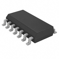
封装信息:提供 SO14 封装,符合 AEC Q100 和 Q003 或同等标准的资格和特性,以及根据 AEC Q001 和 Q002 或同等标准进行的高级筛选。