HD1520FX
HIGH VOLTAGE NPN POWER TRANSISTOR
FOR HIGH DEFINITION CRT DISPLAYS
n
n
STATE-OF-THE-ART TECHNOLOGY:
DIFFUSED COLLECTOR "ENHANCED
GENERATION" EHVS1
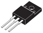
Figure 1: Package
WIDER RANGE OF OPTIMUM DRIVE
CONDITIONS
)
s
(
t
c
u
d
o
)
r
s
(
P
t
c
e
t
u
e
d
l
o
o
r
s
P
b
e
O
t
e
l
)
o
s
(
s
t
b
c
u
O
d
o
)
r
s
P
(
t
c
e
t
u
e
l
d
o
o
r
s
P
b
O
e
t
e
l
o
s
b
O
n
n
LESS SENSITIVE TO OPERATING
TEMPERATURE VARIATION
FULLY INSULATED POWER PACKAGE U.L.
COMPLIANT
ISOWATT218FX
APPLICATIONS
n
HORIZONTAL DEFLECTION FOR LARGE
AND FLAT SCREEN 100 Hz COLOR TVs
Figure 2: Internal Schematic Diagram
DESCRIPTION
The device is manufactured using Diffused
Collector in Planar technology adopting "Enhance
High Voltage Structure" (EHVS1) developed to fit
High-Definition CRT displays.
The new HD product series show improved silicon
efficiency bringing updated performance to the
Horizontal Deflection stage.
Table 1:
Part Number
Marking
Package
Packaging
HD1520FX
HD1520FX
ISOWATT218FX
TUBE
Table 2: Absolute Maximum Ratings
Symbol
Parameter
Value
Unit
VCES
Collector-Emitter Voltage (VBE = 0)
1500
V
VCEO
Collector-Emitter Voltage (IB= 0)
700
V
VEBO
Emitter-Base Voltage (IC= 0)
10
V
Collector Current
15
A
Collector Peak Current (tp < 5ms)
22
A
Base Current
8
A
12
A
64
W
2500
V
IC
ICM
IB
IBM
Base Peak Current (tp < 5ms)
o
Ptot
Total Dissipation at TC = 25 C
Vins
Insulation Withstand Voltage (RMS) from All Three Leads to
External Heatsink
May 2005
Rev. 1
1/8
�HD1520FX
Symbol
Parameter
Value
Tstg
Storage Temperature
TJ
Max. Operating Junction Temperature
Unit
-65 to 150
°C
150
°C
Table 3: Thermal Data
Thermal Resistance Junction-Case
Rthj-case
Max
1.95
o
C/W
Table 4: Electrical Characteristics (Tcase = 25 oC unless otherwise specified)
Symbol
Parameter
Test Conditions
Collector Cut-off Current VCE = 1500 V
(VBE = 0)
V = 1500 V
ICES
Emitter Cut-off Current
Typ.
TC = 125 oC
CE
IEBO
Min.
IC = 100 mA
hFE
IC = 9 A
du
INDUCTIVE LOAD
ts
Storage Time
tf
Fall Time
ete
b
O
s
b
O
2/8
d
o
r
P
e
let
b
O
(s)
VCE = 5 V
so
VCE = 1 V
VCE = 5 V
b
O
-
LBB(on) = 1.9 µH
t
c
u
d
o
r
P
e
t
e
l
o
)-
IB(on) = 1.3 A
o
r
P
mA
VCE(fly) = 1040 V
uc
10
IB = 1.8 A
IC = 9 A
* Pulsed: Pulsed duration = 300 ms, duty cycle ≤ 1.5 %.
l
o
s
IB = 1.8 A
s
(
t
c
IC = 9 A
Pr
l
o
s
Collector-Emitter
IC = 9 A
Saturation Voltage
Base-Emitter Saturation IC = 9 A
Voltage
DC Current Gain
IC = 1 A
VBE(sat)*
ete
IE = 10 mA
(IC = 0 )
VCE(sat)*
2
u
d
o
700
(IB = 0 )
Emitter-Base Voltage
mA
10
(IC = 0)
VEBO
Unit
0.2
(s)
ct
VEB = 5 V
VCEO(sus)* Collector-Emitter
Sustaining Voltage
Max.
µA
V
)
s
t(
V
3
V
1.3
V
26
5
5.5
9.5
fh = 31250 Hz
IB(off) = -4.2 A
3.2
4
µs
VBE(off) = -2.7 V
220
300
ns
�HD1520FX
Figure 3: Safe Operating Area
Figure 6: Derating Curve
)
s
(
t
c
u
d
o
)
r
s
(
P
t
c
e
t
u
e
d
l
o
o
r
s
P
b
e
O
t
e
l
)
o
s
(
s
t
b
c
u
O
d
o
)
r
s
P
(
t
c
e
t
u
e
l
d
o
o
r
s
P
b
O
e
t
e
l
o
s
b
O
Figure 4: Output Chatacterisctics
Figure 7: Reverse Biased SOA
Figure 5: DC Current Gain
Figure 8: DC Current Gain
3/8
�HD1520FX
Figure 9: Collector-Emitter Saturation Voltage
Figure 11: Base-Emitter Saturation Voltage
)
s
(
t
c
u
d
o
)
r
s
(
P
t
c
e
t
u
e
d
l
o
o
r
s
P
b
e
O
t
e
l
)
o
s
(
s
t
b
c
u
O
d
o
)
r
s
P
(
t
c
e
t
u
e
l
d
o
o
r
s
P
b
O
e
t
e
l
o
s
b
O
Figure 10: Power Losses
4/8
Figure 12: Inductive Load Switching Time
�HD1520FX
Figure 13: Power Losses and Inductive Load Switching Test Circuit
)
s
(
t
c
u
d
o
)
r
s
(
P
t
c
e
t
u
e
d
l
o
o
r
s
P
b
e
O
t
e
l
)
o
s
(
s
t
b
c
u
O
d
o
)
r
s
P
(
t
c
e
t
u
e
l
d
o
o
r
s
P
b
O
e
t
e
l
o
s
b
O
Figure 14: Reverse Biased Safe Operating Area Test Circuit
5/8
�HD1520FX
ISOWATT218FX MECHANICAL DATA
DIM.
A
C
D
D1
E
F
F2
G
G1
H
L
L2
L3
L4
L5
L6
L7
N
R
DIA
MIN.
5.30
2.80
3.10
1.80
0.80
0.65
1.80
10.30
mm
TYP.
MAX.
5.70
3.20
3.50
2.20
1.10
0.95
2.20
11.50
MIN.
0.209
0.110
0.122
0.071
0.031
0.026
0.071
0.406
15.70
10.20
23.20
26.70
44.40
4.70
24.70
15.00
2.20
4.20
3.80
0.602
0.354
0.898
1.035
1.701
0.169
0.957
0.575
0.071
0.150
0.134
inch
TYP.
MAX.
0.224
0.126
0.138
0.087
0.043
0.037
0.087
0.453
)
s
(
t
c
u
d
o
)
r
s
(
P
t
c
e
t
u
e
d
l
o
o
r
s
P
b
e
O
t
e
l
)
o
s
(
s
t
b
c
u
O
d
o
)
r
s
P
(
t
c
e
t
u
e
l
d
o
o
r
s
P
b
O
e
t
e
l
o
s
b
O
5.45
15.30
9.0
22.80
26.30
43.20
4.30
24.30
14.60
1.80
3.80
3.40
0.215
- Weight : 5.6 g (typ.)
- Maximum Torque (applied to mounting flange) Recommended: 0.55 Nm; Maximum: 1 Nm
- The side of the dissipator must be flat within 80 µm
6/8
0.618
0.402
0.913
1.051
1.748
0.185
0.972
0.591
0.087
0.165
0.150
�HD1520FX
Figure 5: Revision History
Version
Release Date
27-May-2005
0.1
Change Designator
Initial Release.
)
s
(
t
c
u
d
o
)
r
s
(
P
t
c
e
t
u
e
d
l
o
o
r
s
P
b
e
O
t
e
l
)
o
s
(
s
t
b
c
u
O
d
o
)
r
s
P
(
t
c
e
t
u
e
l
d
o
o
r
s
P
b
O
e
t
e
l
o
s
b
O
7/8
�HD1520FX
)
s
(
t
c
u
d
o
)
r
s
(
P
t
c
e
t
u
e
d
l
o
o
r
s
P
b
e
O
t
e
l
)
o
s
(
s
t
b
c
u
O
d
o
)
r
s
P
(
t
c
e
t
u
e
l
d
o
o
r
s
P
b
O
e
t
e
l
o
s
b
O
Information furnished is believed to be accurate and reliable. However, STMicroelectronics assumes no responsibility for the consequences
of use of such information nor for any infringement of patents or other rights of third parties which may result from its use. No license is granted
by implication or otherwise under any patent or patent rights of STMicroelectronics. Specifications mentioned in this publication are subject
to change without notice. This publication supersedes and replaces all information previously supplied. STMicroelectronics products are not
authorized for use as critical components in life support devices or systems without express written approval of STMicroelectronics.
The ST logo is a registered trademark of STMicroelectronics
All other names are the property of their respective owners
© 2005 STMicroelectronics - All Rights Reserved
STMicroelectronics group of companies
Australia - Belgium - Brazil - Canada - China - Czech Republic - Finland - France - Germany - Hong Kong - India - Israel - Italy - Japan Malaysia - Malta - Morocco - Singapore - Spain - Sweden - Switzerland - United Kingdom - United States of America
www.st.com
8/8
�
很抱歉,暂时无法提供与“HD1520FX”相匹配的价格&库存,您可以联系我们找货
免费人工找货