L165
3A POWER OPERATIONAL AMPLIFIER
s s s s s
OUTPUT CURRENT UP TO 3A LARGE COMMON-MODE AND DIFFERENTIAL MODE RANGES SOA PROTECTION THERMAL PROTECTION ± 18V SUPPLY
Pentawatt V ORDERING NUMBER: L165V
DESCRIPTION The L165 is a monolithic integrated circuit in Pentawatt® package, intended for use as power operational amplifier in a wide range of applications, including servo amplifiers and power supplies. The high gain and high output power capability provide superiore performance wherever an operational amplifier/power booster combination is required. APPLICATION CIRCUITS Figure 1. Gain > 10.
Figure 2. Unity gain configuration.
July 2003
1/9
�L165
ABSOLUTE MAXIMUM RATINGS
Symbol VS V5 V4 V4 V3 Vi Vj Io Ptot Tstg, Tj Supply voltage Upper power transistor VCE Lower power transistor VCE Input voltage Differential input voltage Peak output current (internally limited) Power dissipation at Tcase = 90°C Storage and junction temperature Parameter Value ± 18 36 36 VS ± 15 3.5 20 -40 to 150 V A W °C Unit V V V
PIN CONNECTION (Top view)
SCHEMATIC DIAGRAM
THERMAL DATA
Symbol Rth-j-case Parameter Thermal resistance junction-case max Value 3 Unit °C/W
2/9
�L165
ELECTRICAL CHARACTERISTCS (VS = ± 15 V, Tj = 25 °C unless otherwise specified)
Symbol VS Id Ib Vos Ios SR Parameter Supply Voltage Quiescent Drain Current Input Bias Current Input Offset Voltage Input Offset Current Slew-rate G v = 10 Gv = 1 (°) Vo Output Voltage Swing 8 6 VS = ±18 V Test Condition Min. ±6 40 0.2 ±2 ± 20 Typ. Max. ± 18 60 1 ± 10 ± 200 Unit V mA µA mV nA V/µs
f = 1kHz Ip = 0.3A
Ip = 3A
Vpp
27 24
f = 10kHz Ip = 0.3A
Ip = 3A R Gv eN
iN
Vpp
27 24 100 500 80 2 100 70 KΩ dB µV pA dB
Input Resistance (pin 1) Voltage Gain (open loop) Input Noise Voltage Input Noise Current Common-mode Rejection Supply Voltage Rejection
f = 1 KHz B = 10 to 10 000 Hz f = 1 KHz Rg ≤ 10 KΩ; GV = 30 dB Rg = 22 KΩ; Vripple = 0.5 Vrms fripple = 100 Hz Gv = 10 Gv = 1 00 f = 1 kHz; RL = 4Ω Ip = 1.6 A; Po = 5W Ip = 1.6 A; Po = 18W Ptot = 12 W Ptot = 6 W
CMR SVR
60 40 70 60 110 130
dB dB % % °C °C
Efficiency
Tsd
Thermal Shut-down Case Temperature
3/9
�L165
Figure 3. Open loop frequency response. Figure 6. Maximum output current vs. voltage [VCE] across each output transistor.
Figure 4. Closed loop frequency response (circuit of figure 2).
Figure 7. Safe operating area and collector characteristics of the protected power transistor.
Figure 5. Large signal frequency response.
Figure 8. Maximum allowable power dissipation vs. ambient temperature.
4/9
�L165
Figure 9. Bidirectional DC motor control with TTL/CMOS/µP compatible inputs.
Must be VS2 ≥ VS1; E1, E2 = logic inputs;
VS1 = logic supply voltage
Figure 10. Motor current control circuit with external power transistors (Imotor > 3.5A).
D1 to D4: VF ≤ 1.2 @ I = 4A trr ≤ 500ns Note : The inputvoltage level is compatible with L291 (5-BIT D/A converter). IM R4 The transfer function is: ----- = ----------------Rx R 3 Vi
5/9
�L165
Figure 11. High current tracking regulator.
A: for ± 18 ≤ Vi ± 32 Note: Vz must be chosen in order to verify 2 Vi - Vz ≤ 36V B: for Vi ≤ ±18V
Figure 12. Bidirectional speed control of DC motor (Compensation networks not shown).
D1 to D4: VF ≤ 1.2 @ I = 2A trr ≤ 500ns
6/9
�L165
Figure 13. Split power supply.
Figure 14. Power squarewave oscillator with independent adjustments for frequency and duty-cycle.
P1 : duty-cycle adjust P2 : frequency adjust (f = 700 Hz with C1 = 10 nF, P2 = 100KΩ, f = 25 Hz with C1 = 10 nF, P2 = 0)
7/9
�L165
mm TYP. inch TYP.
DIM. A C D D1 E E1 F F1 G G1 H2 H3 L L1 L2 L3 L4 L5 L6 L7 L9 L10 M M1 V4 V5 Dia
MIN.
2.4 1.2 0.35 0.76 0.8 1.0 3.2 6.6 10.05 17.55 15.55 21.2 22.3 2.6 15.1 6.0 2.1 4.3 4.23 3.75
3.4 6.8
17.85 15.75 21.4 22.5
4.5 4.0
3.65
MAX. MIN. 4.8 1.37 2.8 0.094 1.35 0.047 0.55 0.014 1.19 0.030 1.05 0.031 1.4 0.039 3.6 0.126 7.0 0.260 10.4 10.4 0.396 18.15 0.691 15.95 0.612 21.6 0.831 22.7 0.878 1.29 3.0 0.102 15.8 0.594 6.6 0.236 2.7 0.008 4.8 0.17 4.75 0.167 4.25 0.148 40˚ (typ.) 90˚ (typ.) 3.85 0.144
0.134 0.268
0.703 0.620 0.843 0.886
0.178 0.157
MAX. 0.189 0.054 0.110 0.053 0.022 0.047 0.041 0.055 0.142 0.276 0.409 0.409 0.715 0.628 0.850 0.894 0.051 0.118 0.622 0.260 0.106 0.189 0.187 0.167
OUTLINE AND MECHANICAL DATA
Weight: 2.00gr
Pentawatt V
0.152
L L1 E M1 A C D1 L5 L2 L3 D V5 H2
F E V4 E1
M
H3 Dia. L9 L10 L7 L6 L4 F1 H2 F
G G1
V4
RESIN BETWEEN LEADS
PENTVME
0015981
8/9
�L165
Information furnished is believed to be accurate and reliable. However, STMicroelectronics assumes no responsibility for the consequences of use of such information nor for any infringement of patents or other rights of third parties which may result from its use. No license is granted by implication or otherwise under any patent or patent rights of STMicroelectronics. Specifications mentioned in this publication are subject to change without notice. This publication supersedes and replaces all information previously supplied. STMicroelectronics products are not authorized for use as critical components in life support devices or systems without express written approval of STMicroelectronics. STMicroelectronics acknowledges the trademarks of all companies referred to in this document. The ST logo is a registered trademark of STMicroelectronics © 2003 STMicroelectronics - All Rights Reserved STMicroelectronics GROUP OF COMPANIES Australia - Brazil - Canada - China - Finland - France - Germany - Hong Kong - India - Israel - Italy - Japan -Malaysia - Malta - Morocco Singapore - Spain - Sweden - Switzerland - United Kingdom - United States. http://www.st.com
9/9
�
很抱歉,暂时无法提供与“L165V”相匹配的价格&库存,您可以联系我们找货
免费人工找货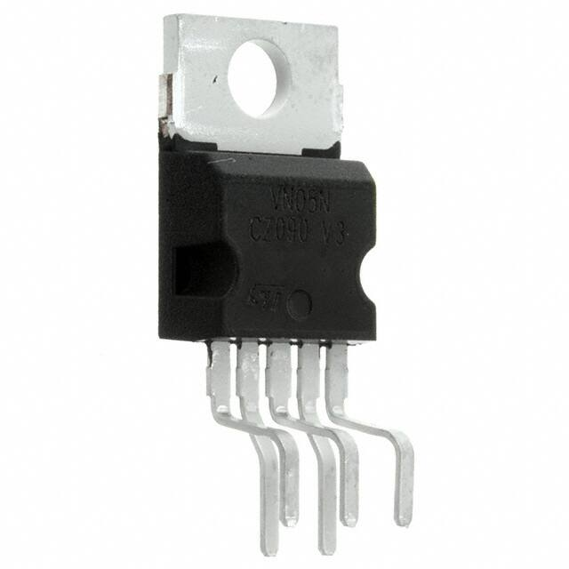


 工商网监
湘ICP备2023018690号
工商网监
湘ICP备2023018690号
