®
L200
ADJUSTABLE VOLTAGE AND CURRENT REGULATOR
ADJUSTABLE OUTPUT CURRENT UP TO 2 A (GUARANTEED UP TO Tj = 150 °C) ADJUSTABLE OUTPUT VOLTAGE DOWN TO 2.85 V INPUT OVERVOLTAGE PROTECTION (UP TO 60 V, 10 ms) SHORT CIRCUIT PROTECTION OUTPUT TRANSISTOR S.O.A. PROTECTION THERMAL OVERLOAD PROTECTION LOW BIAS CURRENT ON REGULATION PIN LOW STANDBY CURRENT DRAIN
Pentawatt®
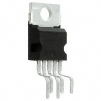
TO-3 (4 lead)
DESCRIPTION The L200 is a monolithic integrated circuit for voltage and current programmable regulation. It is available in Pentawatt® package or 4-lead TO-3 metal case.Current limiting, power limiting, thermal shutdown and input overvoltage protection (up to ABSOLUTE MAXIMUM RATINGS
Symbol Vi Vi ∆Vi-o Io Ptot Tstg Top DC Input Voltage Peak Input Voltage (10 ms) Dropout Voltage Output Current Power Dissipation Storage Temperature Operating Junction Temperature for L200C for L200 Parameter
60 V) make the L200 virtually blow-out proof. The L200 can be used to replace fixed voltage regulators when high output voltage precision is required and eliminates the need to stock a range of fixed voltage regulators.
Value 40 60 32 internally limited internally limited -55 to 150 -25 to 150 -55 to 150
Unit V V V
°C °C °C
THERMAL DATA
TO-3 R th j-case R th j-amb Thermal Resistance Junction-case Thermal Resistance Junction-ambient Max Max 4 °C/W 35 °C/W Pentawatt® 3 °C/W 50 °C/W
January 2000
1/12
�L200
CONNECTION DIAGRAMS AND ORDER CODES (top views)
Type L200 L200 C
Pentawatt®
TO-3 L200 T
L200 CH L200 CV
L200 CT
BLOCK DIAGRAM
APPLICATION CIRCUITS Figure 1. Programmable Voltage Regulator with Current Limiting Figure 2. Programmable Current Regulator.
2/12
�L200
SCHEMATIC DIAGRAM
ELECTRICAL CHARACTERISTICS (Tamb = 25 °C, unless otherwise specified)
Symbol Parameter Test Conditions Min. Typ. Max. Unit
VOLTAGE REGULATION LOOP
Id eN Vo ∆ Vo Vo ∆ Vi ∆ Vo SVR Supply Voltage Rejection Quiescent drain Current (pin 3) Output Noise Voltage Output Voltage Range Voltage Load Regulation (note 1) Line Regulation Vi = 20 V Vo = Vref B = 1 MHz Io = 10 mA ∆Io = 2 A ∆Io = 1.5 A V0 = 5 V Vi = 8 to 18 V V0 = 5 V Io = 500 mA ∆Vi = 10 Vpp f = 100 Hz (note 2) Io = 1.5 A Vi = 20 V ∆V0 ≤ 2% Io = 10 mA 2.64 Io = 10 mA 80 2.85 0.15 0.1 36 1 0.9 4.2 9.2 mA µV V % %
48
60
dB
48
60 2 2.77 2.5 2.86
dB V V
∆Vi-o Vref
Droupout Voltage between Pins 1 and 5 Reference Voltage (pin 4)
3/12
�L200
ELECTRICAL CHARACTERISTICS (continued)
Symbol ∆V ref Parameter Average Temperature Coefficient of Reference Voltage Test Conditions Vi = 20 V Io = 10mA for Tj = - 25 to 125 °C for Tj = 125 to 150 °C Min. Typ. -0.25 -1.5 3 -0.5 10 Max. Unit mV/°C mV/°C µA %/°C
I4 ∆ I4 ∆ T • I4 Zo
Bias Current and Pin 4 Average Temperature Coefficient (pin 4) Output Impedance Vi = 10 V Io = 0.5 A Vo = Vref f = 100 Hz
1.5
mΩ
CURRENT REGULATION LOOP
VSC ∆ VSC ∆ T • VSC ∆ Io Io Current Limit Sense Voltage between Pins 5 and 2 Average Temperature Coefficient of VSC Vi = 10 V I5 = 100 mA Vo = Vref 0.38 0.45 0.03 0.52 V %/°C
Current Load Regulation
Vi = 10 V Io = 0.5 A Io = 1A Io = 1.5 A
∆Vo = 3V
1.4 1 0.9 3.6
% % % A
ISC
Peak Short Circuit Current
Vi - V0 = 14 V (pins 2 and 5 short circuited)
Note 1: A load step of 2 A can be applied provited that input-output differential voltage is lower than 20 V (see Figure 3). Note 2: The same performance can be maintained at higher output levels if a bypassing capacitor is provited between pins 2 and 4.
Figure 3. Typical Safe Operating Area Protection.
Figure 4. Quiescent Current vs. Supply Voltage.
4/12
�L200
Figure 5. Quiescent Current vs. Junction Voltage. Figure 6. Quiescent Current vs. Output Current.
Figure 7. Output Noise Voltage vs. Output Voltage.
Figure 8. Output Noise Voltage vs. Frequency.
Figure 9. Reference Voltage vs. Junction Temperature.
Figure 10. Voltage Load Regulation vs. Junction Temperature.
5/12
�L200
Figure 11. Supply Voltage Rejection vs. Frequency. Figure 12. Dropout Voltage vs. Junction Temperature.
Fi g ur e 1 3 . Ou tpu t I mpe d anc e v s. Frequency.
Figure 14. Output Impedance vs. Output Current.
Figure 15. Voltage Transient Reponse.
Figure 16. Load Transient Reponse.
6/12
�L200
Figure 17. Load Transient Reponse Figure 18. Current Limit Sense Voltage vs. JunctionTemperature.
APPLICATIONS CIRCUITS Figure 19. - Programmable Voltage Regulator Figure 20. - P.C.Board and Components Layout of Figure 19.
Figure 21. - High Current Voltage Regulator with Short Circuit Protection.
Figure 22. - Digitally Selected Regulator with Inhibit.
7/12
�L200
Figure 23. Programmable Voltage and Current Regulator.
Note: Connecting point A to a negative voltage (for example - 3V/10 mA) it is possible to extend the output voltage range down to 0 V and obtain the current limiting down to this level (output short-circuit condition).
Figure 24. High Current Regulator with NPN PassTransistor.
Figure 25. High Current Tracking Regualtor.
8/12
�L200
Figure 26. High Input and Output Voltage. Figure 27. Constant Current Battery Charger.
The resistors R1 and R2 determine the final charging voltage and RSC the initial charging current. D1 prevents discharge of the battery throught the regulator. The resistor RL limits the reverse currents through ther regulator (which should be 100 mA max) when the battery is accidentally reverse connected. If RL is in series with a bulb of 12 V/50 mA rating this will indicate incorrect connection.
Figure 28. 30 W Motor Speed Control.
Figure 29. Loww Turn on.
Figure 30. Light Controller.
9/12
�L200
mm TYP. inch TYP.
DIM. A C D D1 E E1 F F1 G G1 H2 H3 L L1 L2 L3 L4 L5 L6 L7 L9 M M1 V4
MIN.
2.4 1.2 0.35 0.76 0.8 1 3.2 6.6 10.05 17.55 15.55 21.2 22.3 2.6 15.1 6 4.23 3.75
3.4 6.8
17.85 15.75 21.4 22.5
MAX. 4.8 1.37 2.8 1.35 0.55 1.19 1.05 1.4 3.6 7 10.4 10.4 18.15 15.95 21.6 22.7 1.29 3 15.8 6.6
MIN.
0.094 0.047 0.014 0.030 0.031 0.039 0.126 0.260 0.396 0.691 0.612 0.831 0.878 0.102 0.594 0.236
0.2 4.5 4
4.75 0.167 4.25 0.148 40° (typ.)
MAX. 0.189 0.054 0.110 0.053 0.022 0.047 0.041 0.055 0.134 0.142 0.268 0.276 0.409 0.409 0.703 0.715 0.620 0.628 0.843 0.850 0.886 0.894 0.051 0.118 0.622 0.260 0.008 0.177 0.187 0.157 0.167
OUTLINE AND MECHANICAL DATA
Pentawatt V
L L1 L8 V V1 V R A B C D1 L5 L2 L3 D R V4 H2
F E
V4
V3 E R M1
V
V
M
E1
H3 H1 Dia. L7 L6 RESIN BETWEEN LEADS F1 H2 F
G G1
V4
L9
10/12
�L200
mm MIN. A B (*) C D E G N O P R U V 30.1 3.88 12.7 50 ° (typ.) 30 ° (typ.) 26.2 4.20 39.5 1.18 0.15 1.03 0.16 1.55 TYP. 11.8 1 2.5 9.6 20 0.50 0.39 0.098 0.37 0.78 MAX. MIN. inch TYP. 0.46 MAX.
DIM.
OUTLINE AND MECHANICAL DATA
TO3 4-Leads
(*) Measured with Gauge
11/12
�L200
Information furnished is believed to be accurate and reliable.However, STMicroelectronics assumes no responsibility for the consequences of use of such information nor for any infringement of patents or other rights of third parties which may result from its use. No license is granted by implication or otherwise under any patent or patent rights of STMicroelectronics. Specification mentioned in this publication are subject to change without notice. This publication supersedes and replaces all information previous ly supplied. STMicroelectronics products are not authorized for use as critical components in life support devices or systems without express written approval of STMicroelectronics. The ST logo is a registered trademark of STMicroelectronics © 2000 STMicroelectronics – Printed in Italy – All Rights Reserved STMicroelectronics GROUP OF COMPANIES Australia - Brazil - China - Finland - France - Germany - Hong Kong - India - Italy - Japan - Malaysia - Malta - Morocco Singapore - Spain - Sweden - Switzerland - United Kingdom - U.S.A. http://www.st.com
12/12
�
很抱歉,暂时无法提供与“L200CH”相匹配的价格&库存,您可以联系我们找货
免费人工找货