L2G2IS
MEMS motion sensor:
ultra-compact two-axis gyroscope for optical image stabilization
Datasheet - production data
Description
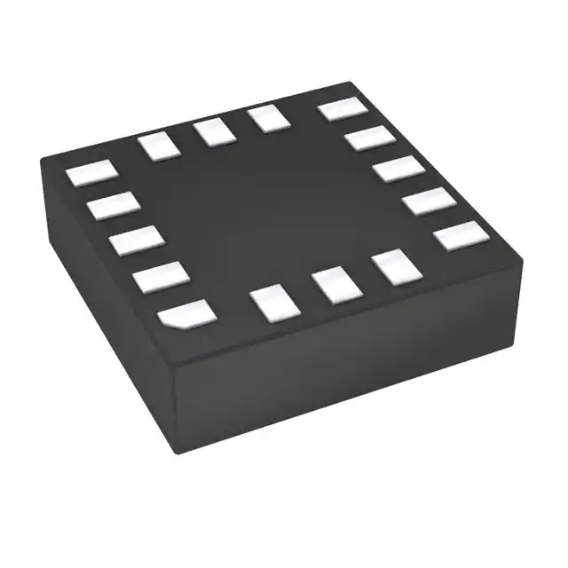
The L2G2IS is a two-axis MEMS gyroscope for
optical image stabilization applications.
It includes a sensing element and an IC interface
capable of providing the measured angular rate to
the application through an SPI digital interface.
The unique sensing element is manufactured
using a dedicated micromachining process
developed by STMicroelectronics to produce
inertial sensors and actuators on silicon wafers.
/*$��������[���[����PP�
Features
±100 dps / ±200 dps full-scale range
Wide supply voltage range: 1.71 V to 3.6 V
Low-voltage compatible IOs
3- and 4-wire SPI digital interface
The IC interface is manufactured using a CMOS
process that allows a high level of integration to
design a dedicated circuit which is trimmed to
better match the characteristics of the sensing
element.
The L2G2IS is available in a plastic land grid
array (LGA) package and can operate over a
temperature range of -40 °C to +85 °C.
Embedded temperature sensor
Embedded self-test
Integrated low- and high-pass filters with userselectable bandwidth
Power-down and sleep modes for smart power
saving
ECOPACK®, RoHS and “Green” compliant
Applications
Optical image stabilization
Table 1. Device summary
Order code
Temperature range (°C)
Package
Packing
L2G2IS
-40 to +85
LGA-16 (2.3x2.3x0.7 mm)
Tray
L2G2ISTR
-40 to +85
LGA-16 (2.3x2.3x0.7 mm)
Tape and reel
February 2016
This is information on a product in full production.
DocID027248 Rev 2
1/26
www.st.com
�Contents
L2G2IS
Contents
1
2
3
Block diagram and pin description . . . . . . . . . . . . . . . . . . . . . . . . . . . . . 6
1.1
System block diagram . . . . . . . . . . . . . . . . . . . . . . . . . . . . . . . . . . . . . . . . 6
1.2
Pin description . . . . . . . . . . . . . . . . . . . . . . . . . . . . . . . . . . . . . . . . . . . . . . 7
Terminology & functionality . . . . . . . . . . . . . . . . . . . . . . . . . . . . . . . . . . . 8
2.1
Sensitivity . . . . . . . . . . . . . . . . . . . . . . . . . . . . . . . . . . . . . . . . . . . . . . . . . . 8
2.2
Zero-rate level . . . . . . . . . . . . . . . . . . . . . . . . . . . . . . . . . . . . . . . . . . . . . . 8
2.3
Data-ready interrupt and synchronous reading . . . . . . . . . . . . . . . . . . . . . 8
2.4
Temperature sensor . . . . . . . . . . . . . . . . . . . . . . . . . . . . . . . . . . . . . . . . . . 8
Mechanical and electrical characteristics . . . . . . . . . . . . . . . . . . . . . . . . 9
3.1
Mechanical characteristics . . . . . . . . . . . . . . . . . . . . . . . . . . . . . . . . . . . . . 9
3.2
Electrical characteristics . . . . . . . . . . . . . . . . . . . . . . . . . . . . . . . . . . . . . . 10
3.3
Temperature sensor characteristics . . . . . . . . . . . . . . . . . . . . . . . . . . . . . 11
3.4
SPI - serial peripheral interface . . . . . . . . . . . . . . . . . . . . . . . . . . . . . . . . 12
3.5
Absolute maximum ratings . . . . . . . . . . . . . . . . . . . . . . . . . . . . . . . . . . . . 13
4
Application hints . . . . . . . . . . . . . . . . . . . . . . . . . . . . . . . . . . . . . . . . . . . 14
5
Digital interfaces . . . . . . . . . . . . . . . . . . . . . . . . . . . . . . . . . . . . . . . . . . . 15
5.1
SPI bus interface . . . . . . . . . . . . . . . . . . . . . . . . . . . . . . . . . . . . . . . . . . . 15
5.1.1
SPI read . . . . . . . . . . . . . . . . . . . . . . . . . . . . . . . . . . . . . . . . . . . . . . . . . 16
5.1.2
SPI write . . . . . . . . . . . . . . . . . . . . . . . . . . . . . . . . . . . . . . . . . . . . . . . . 16
5.1.3
SPI read in 3-wire mode . . . . . . . . . . . . . . . . . . . . . . . . . . . . . . . . . . . . 17
6
Output register mapping . . . . . . . . . . . . . . . . . . . . . . . . . . . . . . . . . . . . 18
7
Register description . . . . . . . . . . . . . . . . . . . . . . . . . . . . . . . . . . . . . . . . 19
2/26
7.1
WHO_AM_I (00h) . . . . . . . . . . . . . . . . . . . . . . . . . . . . . . . . . . . . . . . . . . . 19
7.2
TEMP_OUT_L (01h), TEMP_OUT_H (02h) . . . . . . . . . . . . . . . . . . . . . . . 19
7.3
OUT_X_L (03h), OUT_X_H (04h) . . . . . . . . . . . . . . . . . . . . . . . . . . . . . . 19
7.4
OUT_Y_L (05h), OUT_Y_H (06h) . . . . . . . . . . . . . . . . . . . . . . . . . . . . . . 19
7.5
STATUS_REG (09h) . . . . . . . . . . . . . . . . . . . . . . . . . . . . . . . . . . . . . . . . . 19
DocID027248 Rev 2
�L2G2IS
8
9
Contents
7.6
CTRL_REG1 (0Bh) . . . . . . . . . . . . . . . . . . . . . . . . . . . . . . . . . . . . . . . . . 20
7.7
CTRL_REG2 (0Ch) . . . . . . . . . . . . . . . . . . . . . . . . . . . . . . . . . . . . . . . . . 21
7.8
CTRL_REG3 (0Dh) . . . . . . . . . . . . . . . . . . . . . . . . . . . . . . . . . . . . . . . . . 21
7.9
ORIENT_CONFIG (10h) . . . . . . . . . . . . . . . . . . . . . . . . . . . . . . . . . . . . . 22
7.10
OFF_X (11h) . . . . . . . . . . . . . . . . . . . . . . . . . . . . . . . . . . . . . . . . . . . . . . . 22
7.11
OFF_Y(12h) . . . . . . . . . . . . . . . . . . . . . . . . . . . . . . . . . . . . . . . . . . . . . . . 23
7.12
CTRL_REG4 (1Fh) . . . . . . . . . . . . . . . . . . . . . . . . . . . . . . . . . . . . . . . . . . 23
Package information . . . . . . . . . . . . . . . . . . . . . . . . . . . . . . . . . . . . . . . . 24
8.1
Soldering information . . . . . . . . . . . . . . . . . . . . . . . . . . . . . . . . . . . . . . . . 24
8.2
LGA-16 package . . . . . . . . . . . . . . . . . . . . . . . . . . . . . . . . . . . . . . . . . . . 24
Revision history . . . . . . . . . . . . . . . . . . . . . . . . . . . . . . . . . . . . . . . . . . . 25
DocID027248 Rev 2
3/26
26
�List of tables
L2G2IS
List of tables
Table 1.
Table 2.
Table 3.
Table 4.
Table 5.
Table 6.
Table 7.
Table 8.
Table 9.
Table 10.
Table 11.
Table 12.
Table 13.
Table 14.
Table 15.
Table 16.
Table 17.
Table 18.
Table 19.
Table 20.
Table 21.
Table 22.
Table 23.
Table 24.
Table 25.
Table 26.
Table 27.
Table 28.
Table 29.
Table 30.
Table 31.
Table 32.
Table 33.
Table 34.
Table 35.
4/26
Device summary . . . . . . . . . . . . . . . . . . . . . . . . . . . . . . . . . . . . . . . . . . . . . . . . . . . . . . . . . . 1
Pin description . . . . . . . . . . . . . . . . . . . . . . . . . . . . . . . . . . . . . . . . . . . . . . . . . . . . . . . . . . . 6
Mechanical characteristics . . . . . . . . . . . . . . . . . . . . . . . . . . . . . . . . . . . . . . . . . . . . . . . . . . 8
Electrical characteristics . . . . . . . . . . . . . . . . . . . . . . . . . . . . . . . . . . . . . . . . . . . . . . . . . . . . 9
Temperature sensor characteristics . . . . . . . . . . . . . . . . . . . . . . . . . . . . . . . . . . . . . . . . . . 10
SPI slave timing values. . . . . . . . . . . . . . . . . . . . . . . . . . . . . . . . . . . . . . . . . . . . . . . . . . . . 11
Absolute maximum ratings . . . . . . . . . . . . . . . . . . . . . . . . . . . . . . . . . . . . . . . . . . . . . . . . . 12
External component values. . . . . . . . . . . . . . . . . . . . . . . . . . . . . . . . . . . . . . . . . . . . . . . . . 13
Serial interface pin description . . . . . . . . . . . . . . . . . . . . . . . . . . . . . . . . . . . . . . . . . . . . . . 14
Register address map. . . . . . . . . . . . . . . . . . . . . . . . . . . . . . . . . . . . . . . . . . . . . . . . . . . . . 17
WHO_AM_I register . . . . . . . . . . . . . . . . . . . . . . . . . . . . . . . . . . . . . . . . . . . . . . . . . . . . . . 18
TEMP_OUT_L register . . . . . . . . . . . . . . . . . . . . . . . . . . . . . . . . . . . . . . . . . . . . . . . . . . . . 18
TEMP_OUT_H register. . . . . . . . . . . . . . . . . . . . . . . . . . . . . . . . . . . . . . . . . . . . . . . . . . . . 18
TEMP_OUT resolution . . . . . . . . . . . . . . . . . . . . . . . . . . . . . . . . . . . . . . . . . . . . . . . . . . . . 18
STATUS_REG register . . . . . . . . . . . . . . . . . . . . . . . . . . . . . . . . . . . . . . . . . . . . . . . . . . . . 18
STATUS_REG description . . . . . . . . . . . . . . . . . . . . . . . . . . . . . . . . . . . . . . . . . . . . . . . . . 19
CTRL_REG1 register . . . . . . . . . . . . . . . . . . . . . . . . . . . . . . . . . . . . . . . . . . . . . . . . . . . . . 19
CTRL_REG1 description . . . . . . . . . . . . . . . . . . . . . . . . . . . . . . . . . . . . . . . . . . . . . . . . . . 19
Operating mode selection . . . . . . . . . . . . . . . . . . . . . . . . . . . . . . . . . . . . . . . . . . . . . . . . . . 20
CTRL_REG2 register . . . . . . . . . . . . . . . . . . . . . . . . . . . . . . . . . . . . . . . . . . . . . . . . . . . . . 20
CTRL_REG2 description . . . . . . . . . . . . . . . . . . . . . . . . . . . . . . . . . . . . . . . . . . . . . . . . . . 20
CTRL_REG3 register . . . . . . . . . . . . . . . . . . . . . . . . . . . . . . . . . . . . . . . . . . . . . . . . . . . . . 20
CTRL_REG3 description . . . . . . . . . . . . . . . . . . . . . . . . . . . . . . . . . . . . . . . . . . . . . . . . . . 20
Low-pass filter cutoff frequency selection . . . . . . . . . . . . . . . . . . . . . . . . . . . . . . . . . . . . . . 21
ORIENT_CONFIG register . . . . . . . . . . . . . . . . . . . . . . . . . . . . . . . . . . . . . . . . . . . . . . . . . 21
ORIENT_CONFIG description . . . . . . . . . . . . . . . . . . . . . . . . . . . . . . . . . . . . . . . . . . . . . . 21
OFF_X register . . . . . . . . . . . . . . . . . . . . . . . . . . . . . . . . . . . . . . . . . . . . . . . . . . . . . . . . . . 21
OFF_X description . . . . . . . . . . . . . . . . . . . . . . . . . . . . . . . . . . . . . . . . . . . . . . . . . . . . . . . 21
OFF_Y register . . . . . . . . . . . . . . . . . . . . . . . . . . . . . . . . . . . . . . . . . . . . . . . . . . . . . . . . . . 22
OFF_Y description . . . . . . . . . . . . . . . . . . . . . . . . . . . . . . . . . . . . . . . . . . . . . . . . . . . . . . . 22
CTRL_REG4 register . . . . . . . . . . . . . . . . . . . . . . . . . . . . . . . . . . . . . . . . . . . . . . . . . . . . . 22
CTRL_REG4 description . . . . . . . . . . . . . . . . . . . . . . . . . . . . . . . . . . . . . . . . . . . . . . . . . . 22
High-pass filter cutoff frequency selection . . . . . . . . . . . . . . . . . . . . . . . . . . . . . . . . . . . . . 22
LGA-16 package outer dimensions. . . . . . . . . . . . . . . . . . . . . . . . . . . . . . . . . . . . . . . . . . . 23
Document revision history. . . . . . . . . . . . . . . . . . . . . . . . . . . . . . . . . . . . . . . . . . . . . . . . . . 24
DocID027248 Rev 2
�L2G2IS
List of figures
List of figures
Figure 1.
Figure 2.
Figure 3.
Figure 4.
Figure 5.
Figure 6.
Figure 7.
Figure 8.
Figure 9.
Figure 10.
Block diagram . . . . . . . . . . . . . . . . . . . . . . . . . . . . . . . . . . . . . . . . . . . . . . . . . . . . . . . . . . . . 6
Pin connections . . . . . . . . . . . . . . . . . . . . . . . . . . . . . . . . . . . . . . . . . . . . . . . . . . . . . . . . . . 7
SPI slave timing diagram . . . . . . . . . . . . . . . . . . . . . . . . . . . . . . . . . . . . . . . . . . . . . . . . . . 12
L2G2IS electrical connections and external components . . . . . . . . . . . . . . . . . . . . . . . . . . 14
SPI read protocol . . . . . . . . . . . . . . . . . . . . . . . . . . . . . . . . . . . . . . . . . . . . . . . . . . . . . . . . 16
SPI write protocol . . . . . . . . . . . . . . . . . . . . . . . . . . . . . . . . . . . . . . . . . . . . . . . . . . . . . . . . 16
Multiple byte SPI write protocol (2-byte example). . . . . . . . . . . . . . . . . . . . . . . . . . . . . . . . 17
SPI read protocol in 3-wire mode . . . . . . . . . . . . . . . . . . . . . . . . . . . . . . . . . . . . . . . . . . . . 17
LPF chain block diagram . . . . . . . . . . . . . . . . . . . . . . . . . . . . . . . . . . . . . . . . . . . . . . . . . . 22
LGA-16 package outline and dimensions . . . . . . . . . . . . . . . . . . . . . . . . . . . . . . . . . . . . . . 24
DocID027248 Rev 2
5/26
26
�Block diagram and pin description
L2G2IS
1
Block diagram and pin description
1.1
System block diagram
Figure 1. Block diagram
08;
0(06�6(1625
$FWXDWLRQ�,QWHUIDFH
&��� 9
FRQYHUWHU
)6�6HOHFWLRQ
6/26
DocID027248 Rev 2
6&�ILOWHU
$'&
'LJLWDO
�ILOWHUV
63,
�L2G2IS
Pin description
14
GND
Res
9
(TOP VIEW)
DIRECTIONS OF THE
DETECTABLE
ANGULAR RATES
SDI/SDO
SDO
5
8
Vdd_IO
SCL
CS
6
DRDY
+Ω X
1
BOTTOM
VIEW
Res
Res
16
13
(1)
Res
Res
+Ω Y
Vdd
Reg
Cap
Figure 2. Pin connections
Res
1.2
Block diagram and pin description
1. Leave pin electrically unconnected and soldered to PCB.
Table 2. Pin description
Pin#
Name
1
Vdd_IO
2
SCL
3
SDI/SDO
4
SDO
5
CS
6
DRDY
7
(1)
Res
Function
Power supply for I/O pins
Clock line for SPI interface
Serial data input (SDI)
3-wire interface serial data output (SDO)
Serial data output (SDO)
Chip-select line
Data ready signal
Leave unconnected
8
Res
Connect to GND
9
Res
Connect to GND
10
Res
Connect to GND
11
Res
Connect to GND
12
GND
0 V power supply
13
Res
Connect to GND
14
Cap
Capacitance connection pin for internal charge pump
15
Reg
Capacitance connection pin for internal regulator
16
Vdd
Power supply
1. Leave pin electrically unconnected and soldered to PCB.
DocID027248 Rev 2
7/26
26
�Terminology & functionality
L2G2IS
2
Terminology & functionality
2.1
Sensitivity
An angular rate gyroscope is a device that produces a positive-going digital output for
counterclockwise rotation around the sensitive axis considered. Sensitivity describes the
gain of the sensor and can be determined by applying a defined angular velocity to it. This
value changes very little over temperature and time.
2.2
Zero-rate level
The zero-rate level describes the actual output signal if there is no angular rate present. The
zero-rate level of highly accurate MEMS sensors is, to some extent, a result of stress to the
sensor and therefore the zero-rate level can slightly change after mounting the sensor on a
printed circuit board or after exposing it to extensive mechanical stress. This value changes
very little over temperature and time.
2.3
Data-ready interrupt and synchronous reading
On the L2G2IS the angular rate data can be retrieved using a synchronous read. To perform
a synchronous read, CTRL_REG3 (0Dh) (DRDY_EN) has to be set to '1' in order to enable
the data-ready interrupt on the DRDY pin (refer to Figure 4). To properly perform a
synchronous read, the angular rate data have to be read every time the DRDY pin goes
high.
The DRDY signal can be latched (default condition) or pulsed if the CTRL_REG1 (0Bh)
(P_DRDY) is set to ‘1’. When a latched condition is selected, the interrupt goes low when
the high part of one of the output channels is read (OUT_X_H (04h) or OUT_Y_H (06h)) and
returns high when new data is generated. When a pulsed condition is selected, the interrupt
behavior is independent from the reading operations and remains high for 75 μsec every
time new data is generated. The DRDY pin is set by default as push-pull output, but it can
be configured as open-drain output by setting CTRL_REG3 (0Dh) (PP_OD) to ‘1’.
2.4
Temperature sensor
The temperature data can be retrieved from the TEMP_OUT_L (01h), TEMP_OUT_H (02h)
register, as two’s complement data in 12-bit format left-justified. The output of the
temperature sensor is 0 at 25 °C.
8/26
DocID027248 Rev 2
�L2G2IS
Mechanical and electrical characteristics
3
Mechanical and electrical characteristics
3.1
Mechanical characteristics
Vdd = 2.4 V and T = 25 °C unless otherwise noted(a).
Table 3. Mechanical characteristics
Symbol
Parameter
FS
Measurement range
So
Sensitivity
Test condition
Min.
Typ.(1)
Max.
±100
dps
±200
FS = ±100 dps
262
FS = ±200 dps
131
DVoff
Digital zero-rate level
Rn
Rate noise density(2)
0 - 20 Hz bandwidth
PhDl
Phase delay(3)
At 20 Hz (280 Hz BW selected)
ODR
Digital output data rate
Top
Operating temperature
range
-40
Unit
LSb/dps
±5
dps
0.006
dps Hz
7
deg
9.09
kHz
+85
°C
1. Typical specifications are not guaranteed.
2. Guaranteed by design.
3. Refer to Figure 9: LPF chain block diagram and Table 24: Low-pass filter cutoff frequency selection.
a. The product is factory calibrated at 2.4 V. The operational power supply range is specified in Table 4.
DocID027248 Rev 2
9/26
26
�Mechanical and electrical characteristics
3.2
L2G2IS
Electrical characteristics
@ Vdd = 2.4 V, T = 25 °C unless otherwise noted(b).
Table 4. Electrical characteristics
Symbol
Parameter
Test condition
Min.
Typ.(1)
Max.
Unit
2.4
3.6
V
Vdd
V
Vdd
Supply voltage
1.71
Vdd_IO
I/O pins supply
voltage(2)
1.71
Idd
Supply current in
normal mode
3.8
mA
IddSL
Supply current in
sleep mode(3)
1.85
mA
IddPdn
Supply current in
power-down mode
20
μA
IcapIO
I/O pad driving
current capability
4
mA
VIH
Digital high-level
input voltage
VIL
Digital low-level
input voltage
Top
Operating
temperature range
0.8*Vdd_IO
-40
V
0.2*Vdd_IO
V
+85
°C
1. Typical specifications are not guaranteed.
2. It is possible to remove Vdd maintaining Vdd_IO without blocking the communication busses, in this condition the
measurement chain is powered off.
3. Sleep mode introduces a faster turn-on time relative to power-down mode.
b. The product is factory calibrated at 2.4 V.
10/26
DocID027248 Rev 2
�L2G2IS
3.3
Mechanical and electrical characteristics
Temperature sensor characteristics
@ AVdd = 2.4 V, T = 25 °C unless otherwise noted(c).
Table 5. Temperature sensor characteristics
Symbol
Parameter
TSDr
Temperature sensor
output change vs.
temperature
TODR
Test condition
Min.
Typ.(1)
Max.
Unit
0.0625
°C/digit
Temperature refresh rate
70
Hz
TACC
Temperature absolute
accuracy(2)
±4
°C
Top
Operating temperature
range
-40
+85
°C
1. Typical specifications are not guaranteed.
2. The output of the temperature sensor is 0 at 25 °C. Refer to Section 2.4: Temperature sensor on how to read the
temperature sensor output data.
c. The product is factory calibrated at 2.4 V.
DocID027248 Rev 2
11/26
26
�Mechanical and electrical characteristics
3.4
L2G2IS
SPI - serial peripheral interface
Subject to general operating conditions for Vdd and Top.
Table 6. SPI slave timing values
Value(1)
Symbol
Parameter
Unit
Min
tc(SCL)
SPI clock cycle
fc(SCL)
SPI clock frequency
tsu(CS)
CS setup time
5
th(CS)
CS hold time
8
tsu(SI)
SDI input setup time
5
th(SI)
SDI input hold time
15
tv(SO)
SDO valid output time
th(SO)
SDO output hold time
tdis(SO)
SDO output disable time
Max
100
ns
10
MHz
ns
50
6
50
1. Values are guaranteed at 10 MHz clock frequency for SPI, based on characterization results, not tested in production.
Figure 3. SPI slave timing diagram
&6
&6
W
WWF�6&/�
F�63&�
VX�&6�
WVX�&6�
WK�&6�
WK�&6�
6&/
63&
VX�6,�
WWVX�6,�
6',
6',
WK�6,�
WK�6,�
/6%�,1�
06%�,1�
WWY�62�
Y�62�
6'2
6'2
Note:
12/26
WGLV�62�
WGLV�62�
WK�62�
WK�62�
06%�287
/6%�287
Measurement points are done at 0.2·Vdd_IO and 0.8·Vdd_IO, for both input and output
ports.
DocID027248 Rev 2
�L2G2IS
3.5
Mechanical and electrical characteristics
Absolute maximum ratings
Stresses above those listed as “absolute maximum ratings” may cause permanent damage
to the device. This is a stress rating only and functional operation of the device under these
conditions is not implied. Exposure to maximum rating conditions for extended periods may
affect device reliability.
Table 7. Absolute maximum ratings
Symbol
Vdd
Vdd_IO
Maximum value
Unit
Power supply
-0.3 to 4.8
V
Power supply for I/O pins
-0.3 to Vdd
V
Vin
Input voltage on:
(CS, SDI/SDO, SDO, SCL)
-0.3 to Vdd_IO +0.1
V
TSTG
Storage temperature range
-40 to +125
°C
10,000
g
2 (HBM)
kV
Sg
ESD
Note:
Ratings
Acceleration g for 0.2 ms
Electrostatic discharge protection
Supply voltage on any pin should never exceed 4.8 V.
This device is sensitive to mechanical shock, improper handling can cause
permanent damage to the part.
This device is sensitive to electrostatic discharge (ESD), improper handling can
cause permanent damage to the part.
DocID027248 Rev 2
13/26
26
�Application hints
4
L2G2IS
Application hints
Figure 4. L2G2IS electrical connections and external components
C4
GND GND AVdd
C2
C1
14
GND
1
GND
BOTTOM
VIEW
GND
GND
Vdd_IO
SCL
SDI/SDO
GND
SDO
9
5
8
CS
6
(1)
DRDY
GND
(TOP VIEW)
DIRECTIONS OF THE
DETECTABLE
ANGULAR RATES
16
13
NC
+Ω X
Vdd
GND
Reg
+Ω Y
Cap
C3
1. Leave pin electrically unconnected and soldered to PCB.
Table 8. External component values
Name
Value
Purpose
C1
1 μF
Decoupling
C2
100 pF
Decoupling
10 nF (16 V class)
Charge pump
100 nF (5 V class)
Internal regulator
(1)
C3
C4
1. This value must guarantee a minimum of 1 nF value under 12 V bias condition.
Power supply decoupling capacitors (100 pF + 1 μF) should be placed as near as possible
to the device (common design practice).
14/26
DocID027248 Rev 2
�L2G2IS
5
Digital interfaces
Digital interfaces
The registers embedded inside the L2G2IS may be accessed through the SPI serial
interfaces.
Table 9. Serial interface pin description
Pin name
CS
Chip-select line
SCL
SPI serial port clock
SDI/SDO
SDO
5.1
Pin description
Serial data input (SDI)
3-wire interface serial data output (SDO)
Serial data output (SDO)
SPI bus interface
The SPI is a bus slave. The SPI allows to write and read the registers of the device.
The serial interface connects to applications using 4 wires: CS, SCL, SDI and SDO.
CS is the serial port enable and it is controlled by the SPI master. It goes low at the start of
the transmission and goes back high at the end. SCL is the serial port clock and it is
controlled by the SPI master. It is stopped high when CS is high (no transmission). SDI and
SDO are respectively the serial port data input and output. Those lines are driven at the
falling edge of SCL and should be captured at the rising edge of SCL.
Both the read register and write register commands are completed in 16 clock pulses or in
multiples of 8 in case of multiple read/write bytes. Bit duration is the time between two falling
edges of SCL. The first bit (bit 0) starts at the first falling edge of SCL after the falling edge
of CS while the last bit (bit 15, bit 23, ...) starts at the last falling edge of SCL just before the
rising edge of CS.
bit 0: RW bit. When 0, the data DI(7:0) is written into the device. When 1, the data DO(7:0)
from the device is read. In latter case, the chip will drive SDO at the start of bit 8.
bit 1-7: address AD(6:0). This is the address field of the indexed register.
bit 8-15: data DI(7:0) (write mode). This is the data that is written into the device (MSb first).
bit 8-15: data DO(7:0) (read mode). This is the data that is read from the device (MSb first).
The function and the behavior of SDI and SDO remain unchanged.
DocID027248 Rev 2
15/26
26
�Digital interfaces
5.1.1
L2G2IS
SPI read
Figure 5. SPI read protocol
&6
6&/
6',�6'2
'2� '2� '2� '2� '2� '2� '2� '2�
5:
06 $'� $'� $'� $'� $'� $'�
The SPI read command is performed with 16 clock pulses:
bit 0: READ bit. The value is 1.
bit 1: MS bit. When 0, does not increment the address; when 1, increments the address in
multiple reads.
bit 2-7: address AD(5:0). This is the address field of the indexed register.
bit 8-15: data DO(7:0) (read mode). This is the data that will be read from the device (MSb
first).
A multiple read command is also available.
5.1.2
SPI write
Figure 6. SPI write protocol
&6
6&/
6',�6'2
',� ',� ',� ',� ',� ',� ',� ',�
5:
06 $'� $'� $'� $'� $'� $'�
The SPI write command is performed with 16 clock pulses. A multiple byte write command
is performed by adding blocks of 8 clock pulses to the previous one.
bit 0: WRITE bit. The value is 0.
bit 1: MS bit. When 0, does not increment the address; when 1, increments the address in
multiple writes.
bit 2 -7: address AD(5:0). This is the address field of the indexed register.
bit 8-15: data DI(7:0) (write mode). This is the data that will be written inside the device
(MSb first).
bit 16-... : data DI(...-8). Further data in multiple byte writes.
16/26
DocID027248 Rev 2
�L2G2IS
Digital interfaces
Figure 7. Multiple byte SPI write protocol (2-byte example)
&6
6&/
6',�6'2
',� ',� ',� ',� ',� ',� ',� ',� ',�� ',�� ',�� ',�� ',�� ',�� ',� ',�
5:
06 $'� $'� $'� $'� $'� $'�
5.1.3
SPI read in 3-wire mode
3-wire mode is entered by setting the CTRL_REG1 (0Bh) (SIM) bit equal to ‘1’ (SPI serial
interface mode selection).
Figure 8. SPI read protocol in 3-wire mode
CS
CS
SCL
SPC
SDI/O
SDI/SDO
D O7 D O6 D O5 DO4 DO3 DO2 DO1 DO0
RW
MS
AD5 AD 4 AD 3 AD2 AD1 AD 0
The SPI Read command is performed with 16 clock pulses:
bit 0: READ bit. The value is 1.
bit 1: MS bit. When 0, does not increment the address; when 1, increments the address in
multiple reads.
bit 2-7: address AD(5:0). This is the address field of the indexed register.
bit 8-15: data DO(7:0) (read mode). This is the data that will be read from the device (MSb
first).
A multiple read command is also available in 3-wire mode.
DocID027248 Rev 2
17/26
26
�Output register mapping
6
L2G2IS
Output register mapping
The table given below provides a listing of the 8-bit registers embedded in the device and
the related addresses.
Table 10. Register address map
Name
Type
Register
address
[Hex]
Default
[Hex]
WHO_AM_I
r
00
D9
TEMP_OUT_L
r
01
output
TEMP_OUT_H
r
02
output
OUT_X_L
r
03
output
OUT_X_H
r
04
output
OUT_Y_L
r
05
output
OUT_Y_H
r
06
output
Reserved
--
07-08
--
STATUS_REG
r
09
output
Reserved
--
0A
--
CTRL_REG1
r/w
0B
00
CTRL_REG2
r/w
0C
00
CTRL_REG3
r/w
0D
00
--
0E-0F
--
ORIENT_CONFIG
r/w
10
00
OFF_X
r/w
11
00
OFF_Y
r/w
12
00
--
13-1E
--
r/w
1F
00
Reserved
Reserved
CTRL_REG4
Comment
Reserved
Reserved
Reserved
Registers marked as Reserved must not be changed. Writing to those registers may cause
permanent damage to the device.
To guarantee the proper behavior of the device, all register addresses not listed in the above
table must not be accessed and the content stored in those registers must not be changed.
The content of the registers that are loaded at boot should not be changed. They contain the
factory calibration values. Their content is automatically restored when the device is
powered up.
18/26
DocID027248 Rev 2
�L2G2IS
7
Register description
Register description
The device contains a set of registers which are used to control its behavior and to retrieve
angular rate data. The register address, consisting of 7 bits, is used to identify them and to
write the data through the serial interface.
7.1
WHO_AM_I (00h)
Table 11. WHO_AM_I register
1
7.2
1
0
1
1
0
0
1
0
0
Temp5
Temp4
TEMP_OUT_L (01h), TEMP_OUT_H (02h)
Table 12. TEMP_OUT_L register
Temp3
Temp2
Temp1
Temp0
0
0
Table 13. TEMP_OUT_H register
Temp11
Temp10
Temp9
Temp8
Temp7
Temp6
Table 14. TEMP_OUT resolution
Temp11-Temp0
7.3
Temperature data.
Refer to: Section 2.4: Temperature sensor on how to read the temperature
sensor output data.
OUT_X_L (03h), OUT_X_H (04h)
X-axis angular rate data. The value is expressed as two’s complement.
7.4
OUT_Y_L (05h), OUT_Y_H (06h)
Y-axis angular rate data. The value is expressed as two’s complement.
7.5
STATUS_REG (09h)
Table 15. STATUS_REG register
YXOR
XOR
YOR
0
DocID027248 Rev 2
YXDA
XDA
YDA
0
19/26
26
�Register description
L2G2IS
Table 16. STATUS_REG description
7.6
YXOR
X-, Y-axis data overrun.
(0: no overrun has occurred; 1: new data has overwritten the previous data before it was
read)
XOR
X-axis data overrun.
(0: no overrun has occurred; 1: new data for the X-axis has overwritten the previous data)
YOR
Y-axis data overrun.
(0: no overrun has occurred; 1: new data for the Y-axis has overwritten the previous data)
YXDA
X-, Y-axis new data available.
(0: a new set of data is not yet available; 1: a new set of data is available)
XDA
X-axis new data available.
(0: new data for the X-axis is not yet available; 1: new data for the X-axis is available)
YDA
Y-axis new data available.
(0: new data for the Y-axis is not yet available;1: new data for the Y-axis is available)
CTRL_REG1 (0Bh)
Table 17. CTRL_REG1 register
BOOT
P_DRDY
BLE
SIM
ODU
0(1)
PW1
PW0
1. This bit must be set to ‘0’ for proper operation of the device.
Table 18. CTRL_REG1 description
BOOT
Reboot memory content. Default value: 0
(0: normal mode; 1: reboot memory content(1))
P_DRDY
DRDY signal pulsed. Default value: 0
(0: DRDY is latched; 1: DRDY is pulsed)
BLE
Big/little endian data selection. Default value: 0
(0: Data LSB @ lower address; 1: Data MSB @ lower address)
SIM
SPI Serial Interface Mode selection. Default value: 0
(0: 4-wire interface; 1: 3-wire interface).
ODU
Output data update. Default value: 0
(0: output registers not updated until MSB and LSB have been read;
1: output registers updated continuously)
PW[1:0]
Operating mode selection. Default value: 00
Refer to Table 19: Operating mode selection.
1. Boot request is executed as soon as internal oscillator is turned-on. It is possible to set this bit while in
power-down mode, in this case it will be served at the next normal mode or sleep mode.
20/26
DocID027248 Rev 2
�L2G2IS
Register description
Table 19. Operating mode selection
7.7
PW1
PW0
Operating mode selection
0
0
Power-down
0
1
Power-down
1
0
Sleep mode
1
1
Normal mode
CTRL_REG2 (0Ch)
Table 20. CTRL_REG2 register
LPF_O
0
(1)
0(1)
0(1)
0(1)
HPreset
SWreset
HPF
1. These bits must be set to ‘0’ for proper operation of the device.
Table 21. CTRL_REG2 description
7.8
LPF_O
Low-pass filter order selection. Default value: 0
(0: 2nd order; 1: 1st order).
Refer to Figure 9: LPF chain block diagram and Table 24: Low-pass filter cutoff frequency selection
HPreset
High-pass filter reset. Default value: 0
(1: HPF reset on X and Y-axis)
SWreset
Software reset. Default value: 0
(1: all the configuration register values are restored to default values).
HPF
High-pass filter enable. Default value: 0
(0: high-pass filter is disabled; 1: high-pass filter is enabled)
CTRL_REG3 (0Dh)
Table 22. CTRL_REG3 register
0(1)
ST
0(1)
PP_OD
0(1)
0(1)
DRDY _EN
LPF_D
1. These bits must be set to ‘0’ for proper operation of the device.
Table 23. CTRL_REG3 description
ST
Self-test enable. Default value: 0
(0: Self-test disabled; 1: Self-test enabled)
PP_OD
DRDY pin configuration. Default value: 0
(0: push-pull; 1: open drain)
DRDY_EN
Data ready enable on DRDY pin. Default: 0
(1: DRDY on pin). Section 2.3: Data-ready interrupt and synchronous reading.
LPF_D
Digital low-pass filter enable. Default value: 0
(0: digital low-pass filter disabled; 1: digital low-pass filter enabled).
Refer to Figure 9: LPF chain block diagram and Table 24: Low-pass filter cutoff
frequency selection.
DocID027248 Rev 2
21/26
26
�Register description
L2G2IS
Figure 9. LPF chain block diagram
�
'DWD5HJ
$QDORJ
/3)
'LJLWDO
/3)
$'&
�
/3)B'
/3)B2
Table 24. Low-pass filter cutoff frequency selection
LPF_O (CTRL_REG2 (0Ch))
7.9
LPF_D (CTRL_REG3 (0Dh))
BW (Hz)
Phase delay @ 20 Hz
0
0
280
7 deg (default)
0
1
140
13.5 deg
1
0
350
5 deg
1
1
150
11.5 deg
ORIENT_CONFIG (10h)
Table 25. ORIENT_CONFIG register
0(1)
0(1)
Sign_x
0(1)
Sign_y
0(1)
0(1)
Orient
1. These bits must be set to ‘0’ for proper operation of the device.
Table 26. ORIENT_CONFIG description
7.10
Sign_x
X-axis angular rate sign. Default value: 0
(0: sign unvaried; 1: sign inverted)
Sign_y
Y-axis angular rate sign. Default value: 0
(0: sign unvaried; 1: sign inverted)
Orient
Directional orientation selection. Default value: 0
(0: X-axis - Y-axis; 1: Y-axis - X-axis)
OFF_X (11h)
Table 27. OFF_X register
OFFX7
OFFX6
OFFX5
OFFX4
OFFX3
OFFX2
OFFX1
OFFX0
Table 28. OFF_X description
OFFX[7:0]
22/26
User offset correction register for X-axis. Default value: 0000 0000
The value is expressed as two’s complement.
DocID027248 Rev 2
�L2G2IS
7.11
Register description
OFF_Y(12h)
Table 29. OFF_Y register
OFFY7
OFFY6
OFFY5
OFFY4
OFFY3
OFFY2
OFFY1
OFFY0
Table 30. OFF_Y description
OFFY[7:0]
7.12
User offset correction register for Y-axis. Default value: 0000 0000
The value is expressed as two’s complement.
CTRL_REG4 (1Fh)
Table 31. CTRL_REG4 register
0(1)
0(1)
0(1)
0(1)
FS
0(1)
0(1)
HPF_BW
1. These bits must be set to ‘0’ for proper operation of the device.
Table 32. CTRL_REG4 description
FS
Full-scale selection. Default value: 0
(0: ±100 dps; 1: ±200 dps)
HPF_BW
Digital high-pass filter cutoff frequency selection. Default value: 0
Refer to Table 33: High-pass filter cutoff frequency selection
Table 33. High-pass filter cutoff frequency selection
HPF_BW0
HP cutoff frequency selection
0
0.02 Hz
1
0.09 Hz
DocID027248 Rev 2
23/26
26
�Package information
8
L2G2IS
Package information
In order to meet environmental requirements, ST offers these devices in different grades of
ECOPACK® packages, depending on their level of environmental compliance. ECOPACK®
specifications, grade definitions and product status are available at: www.st.com.
ECOPACK® is an ST trademark.
8.1
Soldering information
The LGA package is compliant with the ECOPACK®, RoHS and “Green” standard.
It is qualified for soldering heat resistance according to JEDEC J-STD-020.
Leave “Pin 1 Indicator” unconnected during soldering.
Land pattern and soldering recommendations are available at www.st.com/mems.
8.2
LGA-16 package
Figure 10. LGA-16 package outline and dimensions
�������B'
Table 34. LGA-16 package outer dimensions
Item
Dimension [mm]
Tolerance [mm]
Length [L]
2.30
±0.1
Width [W]
2.30
±0.1
Height [H]
0.70
MAX
24/26
DocID027248 Rev 2
�L2G2IS
9
Revision history
Revision history
Table 35. Document revision history
Date
Revision
Changes
16-Mar-2015
1
Initial release
17-Feb-2016
2
Added footnote to pin 7 in Figure 2, Table 2, and Figure 4
Updated Section 2.3: Data-ready interrupt and synchronous reading
Updated Sg in Table 7: Absolute maximum ratings
DocID027248 Rev 2
25/26
26
�L2G2IS
IMPORTANT NOTICE – PLEASE READ CAREFULLY
STMicroelectronics NV and its subsidiaries (“ST”) reserve the right to make changes, corrections, enhancements, modifications, and
improvements to ST products and/or to this document at any time without notice. Purchasers should obtain the latest relevant information on
ST products before placing orders. ST products are sold pursuant to ST’s terms and conditions of sale in place at the time of order
acknowledgement.
Purchasers are solely responsible for the choice, selection, and use of ST products and ST assumes no liability for application assistance or
the design of Purchasers’ products.
No license, express or implied, to any intellectual property right is granted by ST herein.
Resale of ST products with provisions different from the information set forth herein shall void any warranty granted by ST for such product.
ST and the ST logo are trademarks of ST. All other product or service names are the property of their respective owners.
Information in this document supersedes and replaces information previously supplied in any prior versions of this document.
© 2016 STMicroelectronics – All rights reserved
26/26
DocID027248 Rev 2
�