®
L4940 series
VERY LOW DROP 1.5 A REGULATORS
s s
s s s s
PRECISE 5 V, 8.5 V, 10 V, 12 V OUTPUTS LOW DROPOUT VOLTAGE (500 mV typ at 1.5A) VERY LOW QUIESCENT CURRENT THERMAL SHUTDOWN SHORT CIRCUIT PROTECTION REVERSE POLARITY PROTECTION
DESCRIPTION The L4940 series of three terminal positive regulators is available in TO-220 and D2PAK package and with several fixed output voltages, making it useful in a wide range of industrial and consumer applications. Thanks to its very low input/output voltage drop, these devices are particularly suitable for battery powered equipments, reducing consumption and prolonging battery life. Each type employs internal current limiting, antisaturation circuit, thermal shut-down and safe area protection.
TO-220
D PAK TO-263
2
BLOCK DIAGRAM
November 1999
1/13
�L4940 series
PIN CONNECTION AND ORDER CODES
ORDERING NUMBERS TO-220 L4940V5 L4940V85 L4940V10 L4940V12 D PAK L4940D2T5 L4940D2T85 L4940D2T10 L4940D2T12
2
OUTPUT VOLTAGE 5V 8.5V 10V 12V
ABSOLUTE MAXIMUM RATING
Symbol VI V IR Forward Input Voltage Reverse Input Voltage VO = 5 V VO = 10 V VO = 12 V IO P tot Output Current Power Dissipation RO = 100 Ω RO = 200 Ω RO = 240 Ω Internally Limited Internally Limited -40 to 150
o
Description
Values 30 -15
Unit V V
VO = 8.5 V RO = 180 Ω
T j , T st g Junction and Storage Temperature
C
THERMAL DATA
Symbol Description Value TO-220 R thj- ca s e Thermal Resistance Junction-case Max R thj-a mb Thermal Resistance Junction-ambient Max 3 50 D PAK 3 62.5
o o 2
Unit
C/W C/W
2/13
�L4940 series
TEST CIRCUITS Figure 1 : DC Parameter.
Figure 2 : Load Rejection.
Figure 3 : Ripple Rejection.
3/13
�L4940 series
ELECTRICAL CHARACTERISTICS FOR L4940V5 (refer to the test circuits, Tj = 25 oC, Vi = 7V, Ci = 0.1 µF, Co = 22 µF unless otherwise specified)
Symbol Vo Vo Vi ∆V o ∆V o IQ ∆IQ ∆ Vo ∆T SVR Vd Is c Parameter Output Voltage Output Voltage Operating Input Voltage Line Regulation Load Regulation Quiescent Current Quiescent Current Change Output Voltage Drift Supply Voltage Rejection Dropout Voltage Short Circuit Current Io = 1 A Io = 0.5 A Io = 1.5 A Vi = 14 V Vi = 6.5 V f = 120 Hz 58 Test Conditions Io = 500 mA Io = 5 mA to 1500 mA Vi = 6.5 to 16 V Io = 5 mA Io = 5 mA Vi = 6 to 17 V 4 8 5 5 30 Min. 4.9 4.8 Typ. 5 5 Max. 5.1 5.2 17 10 25 15 8 50 3 15 0.5 68 200 500 2 2.2 400 900 2.7 2.9 Unit V V V mV mV mA mA mV/ oC dB mV A
Io = 5 to 1500 mA Io = 500 to 1000 mA Io = 5 mA Io = 1.5 A Vi = 6.5 V Io = 5 mA Io = 1.5 A Vi = 6.5 to 16 V
ELECTRICAL CHARACTERISTICS FOR L4940V85 (refer to the test circuits, T j = 25 oC, Vi = 10.5V, Ci = 0.1 µF, Co = 22 µF unless otherwise specified)
Symbol Vo Vo Vi ∆V o ∆V o IQ ∆IQ ∆ Vo ∆T SVR Vd Is c Parameter Output Voltage Output Voltage Operating Input Voltage Line Regulation Load Regulation Quiescent Current Quiescent Current Change Output Voltage Drift Supply Voltage Rejection Dropout Voltage Short Circuit Current Io = 1 A Io = 0.5 A Io = 1.5 A Vi = 14 V Vi = 10.2 V f = 120 Hz 58 Test Conditions Io = 500 mA Io = 5 mA to 1500 mA Vi = 10.2 to 16 V Io = 5 mA Io = 5 mA Vi = 9.5 to 17 V 4 12 8 4 30 Min. 8.3 8.15 Typ. 8.5 8.5 Max. 8.7 8.85 17 9 30 16 8 50 2.5 15 0.8 66 200 500 2 2.2 400 900 2.7 2.9 Unit V V V mV mV mA mA mV/ oC dB mV A
Io = 5 to 1500 mA Io = 500 to 1000 mA Io = 5 mA Io = 1.5 A Vi = 10.2 V Io = 5 mA Io = 1.5 A Vi = 10.2 to 16 V
4/13
�L4940 series
ELECTRICAL CHARACTERISTICS FOR L4940V10 (refer to the test circuits, T j = 25 oC, Vi = 12V, Ci = 0.1 µF, Co = 22 µF unless otherwise specified)
Symbol Vo Vo Vi ∆V o ∆V o IQ ∆IQ ∆ Vo ∆T SVR Vd Is c Parameter Output Voltage Output Voltage Operating Input Voltage Line Regulation Load Regulation Quiescent Current Quiescent Current Change Output Voltage Drift Supply Voltage Rejection Dropout Voltage Short Circuit Current Io = 1 A Io = 0.5 A Io = 1.5 A Vi = 14 V Vi = 11.7 V f = 120 Hz 56 Test Conditions Io = 500 mA Io = 5 mA to 1500 mA Vi = 11.7 to 16 V Io = 5 mA Io = 5 mA Vi = 11 to 17 V 3 15 10 4 30 Min. 9.8 9.6 Typ. 10 10 Max. 10.2 10.4 17 8 35 20 8 50 2 13 1 62 200 500 2 2.2 400 900 2.7 2.9 Unit V V V mV mV mA mA mV/ oC dB mV A A
Io = 5 to 1500 mA Io = 500 to 1000 mA Io = 5 mA Io = 1.5 A Vi = 11.7 V Io = 5 mA Io = 1.5 A Vi = 11.7 to 16 V
ELECTRICAL CHARACTERISTICS FOR L4940V12 (refer to the test circuits, T j = 25 oC, Vi = 14V, Ci = 0.1 µF, Co = 22 µF unless otherwise specified)
Symbol Vo Vo Vi ∆V o ∆V o IQ ∆IQ ∆ Vo ∆T SVR Vd Is c Zo Parameter Output Voltage Output Voltage Operating Input Voltage Line Regulation Load Regulation Quiescent Current Quiescent Current Change Output Voltage Drift Supply Voltage Rejection Dropout Voltage Short Circuit Current Output Impedance Io = 1 A Io = 0.5 A Io = 1.5 A Vi = 14 V f = 1KHz Io = 0.5A f = 120 Hz 55 Test Conditions Io = 500 mA Io = 5 mA to 1500 mA Vi = 13.8 to 17 V Io = 5 mA Io = 5 mA Vi = 13 to 17 V 3 15 10 4 30 Min. 11.75 11.5 Typ. 12 12 Max. 12.25 12.5 17 7 35 25 8 50 1.5 10 1.2 61 200 500 2 40 400 900 2.7 Unit V V V mV mV mA mA mV/ oC dB mV A mΩ
Io = 5 to 1500 mA Io = 500 to 1000 mA Io = 5 mA Io = 1.5 A Vi = 13.8 V Io = 5 mA Io = 1.5 A Vi = 13.8 to 16 V
5/13
�L4940 series
Figure 4 : Dropout voltage vs. Output Current. Figure 5 : Dropout Voltage vs. Temperature.
Figure 6 : Output voltage vs. Temperature (L4940V5).
Figure 7 : Output Voltage vs. Temperature (L4940V85).
Figure 8 : Output voltage vs. Temperature (L4040V10).
Figure 9 : Output Voltage vs. Temperature (L4940V12).
6/13
�L4940 series
Figure 10 : Quiescent Current vs. Temperature (L4940V5). Figure 11 : Quiescent Current vs. Input Voltage (L4940V5).
Figure 12 : Quiescent Current vs. Output Current (L4940V5).
Figure 13 : Short-circuit Current vs. Temperature (L4940V5).
Figure 14 : Peak Output Current vs. Input/OutputDifferential Voltage (L4940V5).
Figure 15 : Low Voltage Behavior (L4940V5 ).
7/13
�L4940 series
Figure 16 : Low Voltage Behavior (L4940V85). Figure 17 : Low Voltage Behavior (L4940V10).
Figure 18 : Low Voltage Behavior (L4940V12).
Figure 19 : Supply Voltage Rejection vs. Frequency (L4940V5).
Figure 20 : Supply Voltage Rejection vs. output Current.
Figure 21 : Load Dump Characteristics (L4940V5 ).
8/13
�L4940 series
Figure 22 : Line Transient Response (L4940V5). Figure 23 : Load Transient Response.
Figure 24 : Total Power Dissipation.
Figure 25 : Distributed Supply with On-card L4940 and L4941 Low-drop Regulators.
9/13
�L4940 series
Figure 26 : Distributed Supply with On-card L4940 and L4941 Low-drop Regulators.
ADVANTAGES OF THESE APPLICATIONS ARE : On card regulation with short-circuit and thermal protection on each output. Very high total system efficiency due to the switching preregulation and very low-drop postregulations.
Figure 27.
ADVANTAGES OF THIS CONFIGURATION ARE : Very high regulation (line and load) on both the output voltages. 12 V output short-circuit and thermally protected. Very high efficiency on the 12 V output due to the very low drop regulator.
10/13
�L4940 series
TO-220 MECHANICAL DATA
DIM. MIN. A C D D1 E F F2 G H2 H3 L2 L3 L5 L6 L7 Dia. 26.3 2.6 15.1 6 3.65 10.05 16.2 26.7 27.1 3 15.8 6.6 3.85 1.035 0.102 0.594 0.236 0.144 2.4 1.2 0.35 0.61 1.15 4.95 5.08 mm TYP. MAX. 4.8 1.37 2.8 1.35 0.55 0.94 1.4 5.21 10.4 10.4 0.396 0.638 1.051 1.067 0.118 0.622 0.260 0.152 0.094 0.047 0.014 0.024 0.045 0.195 0.200 MIN. inch TYP. MAX. 0.189 0.054 0.110 0.053 0.022 0.037 0.055 0.205 0.409 0.409
P011D
11/13
�L4940 series
TO-263 (D2PAK) MECHANICAL DATA
mm MIN. A A1 B B2 C C2 D E G L L2 L3 4.4 2.49 0.7 1.14 0.45 1.23 8.95 10 4.88 15 1.27 1.4 TYP. MAX. 4.6 2.69 0.93 1.7 0.6 1.36 9.35 10.4 5.28 15.85 1.4 1.75 MIN. 0.173 0.098 0.027 0.044 0.017 0.048 0.352 0.393 0.192 0.590 0.050 0.055 inch TYP. MAX. 0.181 0.106 0.036 0.067 0.023 0.053 0.368 0.409 0.208 0.624 0.055 0.068
DIM.
D A C A2 DETAIL”A” A1 B2 B G
C2
DETAIL”A”
E
L2
L
L3
P011P6/F
12/13
�L4940 series
Information furnished is believed to be accurate and reliable. However, STMicroelectronic s assumes no responsibility for the consequences of use of such information nor for any infringement of patents or other rights of third parties which may result from its use. No license is granted by implication or otherwise under any patent or patent rights of STMicroelectronics. Specification mentioned in this publication are subject to change without notice. This publication supersedes and replaces all information previously supplied. STMicroelectronics products are not authorized for use as critical components in life support devices or systems withoutexpress written approval of STMicroelectronics. The ST logo is a registered trademark of STMicroelectronics © 1999 STMicroelectronics – Printed in Italy – All Rights Reserved STMicroelectronics GROUP OF COMPANIES Australia - Brazil - China - Finland - France - Germany - Hong Kong - India - Italy - Japan - Malaysia - Malta - Morocco Singapore - Spain - Sweden - Switzerland - United Kingdom - U.S.A. http://www.st.com .
13/13
�
很抱歉,暂时无法提供与“L4940D2T5”相匹配的价格&库存,您可以联系我们找货
免费人工找货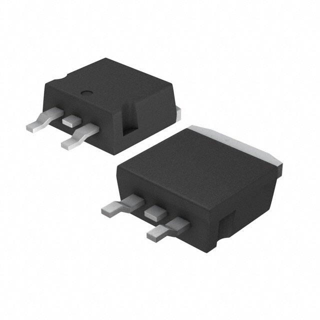


 工商网监
湘ICP备2023018690号
工商网监
湘ICP备2023018690号
