L6226Q
DMOS dual full bridge driver
Features
■
Operating supply voltage from 8 to 52 V
■
2.8 A output peak current (1.4 A DC)
■
RDS(on) 0.73 Ω typ. value @ TJ = 25 °C
■
Operating frequency up to 100 kHz
■
Programmable high side overcurrent detection
and protection
■
Diagnostic output
■
Paralleled operation
■
Cross conduction protection
■
Thermal shutdown
■
Under voltage lockout
■
Integrated fast free wheeling diodes
The L6226Q is a DMOS dual full bridge designed
for motor control applications, realized in
BCDmultipower technology, which combines
isolated DMOS power transistors with CMOS and
bipolar circuits on the same chip. Available in
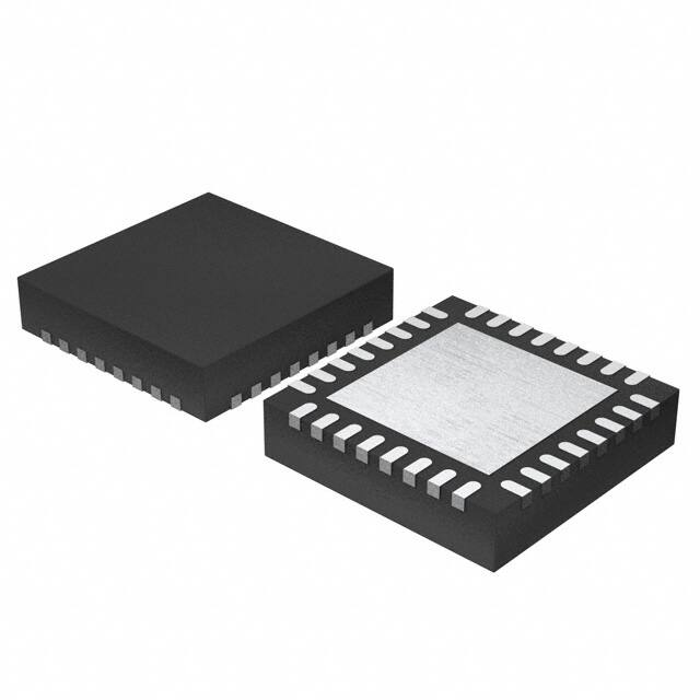
QFN32 5x5 package, the L6226Q features
thermal shutdown and a non-dissipative
overcurrent detection on the high side power
MOSFETs plus a diagnostic output that can be
easily used to implement the overcurrent
protection.
Applications
■
Description
Bipolar stepper motor
■
Dual or quad DC motor
Figure 1.
Block diagram
VBOOT
VBOOT
VBOOT
VCP
VSA
VBOOT
CHARGE
PUMP
PROGCLA
OCDA
OCDA
OVER
CURRENT
DETECTION
OUT1A
10V
THERMAL
PROTECTION
OUT2A
10V
GATE
LOGIC
ENA
IN1A
SENSEA
IN2A
VOLTAGE
REGULATOR
10V
5V
BRIDGE A
OCDB
OCDB
OVER
CURRENT
DETECTION
VSB
PROGCLB
ENB
OUT1B
OUT2B
GATE
LOGIC
SENSEB
IN1B
IN2B
BRIDGE B
D99IN1088A
August 2010
Doc ID 14335 Rev 5
1/29
www.st.com
29
�Contents
L6226Q
Contents
1
Electrical data . . . . . . . . . . . . . . . . . . . . . . . . . . . . . . . . . . . . . . . . . . . . . . 3
1.1
Absolute maximum ratings . . . . . . . . . . . . . . . . . . . . . . . . . . . . . . . . . . . . . 3
1.2
Recommended operating conditions . . . . . . . . . . . . . . . . . . . . . . . . . . . . . 3
1.3
Thermal data . . . . . . . . . . . . . . . . . . . . . . . . . . . . . . . . . . . . . . . . . . . . . . . 4
2
Pin connection . . . . . . . . . . . . . . . . . . . . . . . . . . . . . . . . . . . . . . . . . . . . . . 5
3
Electrical characteristics . . . . . . . . . . . . . . . . . . . . . . . . . . . . . . . . . . . . . 7
4
Circuit description . . . . . . . . . . . . . . . . . . . . . . . . . . . . . . . . . . . . . . . . . . 10
4.1
Power stages and charge pump . . . . . . . . . . . . . . . . . . . . . . . . . . . . . . . . 10
4.2
Logic inputs . . . . . . . . . . . . . . . . . . . . . . . . . . . . . . . . . . . . . . . . . . . . . . . 11
4.3
Truth table . . . . . . . . . . . . . . . . . . . . . . . . . . . . . . . . . . . . . . . . . . . . . . . . . 12
4.4
Non-dissipative overcurrent detection and protection . . . . . . . . . . . . . . . 12
4.5
Thermal protection . . . . . . . . . . . . . . . . . . . . . . . . . . . . . . . . . . . . . . . . . . 16
5
Application information . . . . . . . . . . . . . . . . . . . . . . . . . . . . . . . . . . . . . 17
6
Paralleled operation . . . . . . . . . . . . . . . . . . . . . . . . . . . . . . . . . . . . . . . . 19
7
Output current capability and IC power dissipation . . . . . . . . . . . . . . 23
8
Thermal management . . . . . . . . . . . . . . . . . . . . . . . . . . . . . . . . . . . . . . . 24
9
Package mechanical data . . . . . . . . . . . . . . . . . . . . . . . . . . . . . . . . . . . . 25
10
Order codes . . . . . . . . . . . . . . . . . . . . . . . . . . . . . . . . . . . . . . . . . . . . . . . 27
11
Revision history . . . . . . . . . . . . . . . . . . . . . . . . . . . . . . . . . . . . . . . . . . . 28
2/29
Doc ID 14335 Rev 5
�L6226Q
Electrical data
1
Electrical data
1.1
Absolute maximum ratings
Table 1.
Absolute maximum ratings
Symbol
Parameter
VS
VOD
OCDA,OCDB
PROGCLA,
PROGCLB
VBOOT
VIN,VEN
Parameter
VSA = VSB = VS
60
V
Differential voltage between
VSA, OUT1A, OUT2A, SENSEA and
VSB, OUT1B, OUT2B, SENSEB
VSA = VSB = VS = 60 V,
VSENSEA = VSENSEB = GND
60
V
OCD pins voltage range
-0.3 to + 10
V
PROGCL pins voltage range
-0.3 to + 7
V
VS + 10
V
-0.3 to + 7
V
-1 to + 4
V
VSA = VSB = VS,
tPULSE < 1 ms
3.55
A
RMS supply current (for each VS pin) VSA = VSB = VS
1.4
A
-40 to 150
°C
Bootstrap peak voltage
VSA = VSB = VS
Input and enable voltage range
Voltage range at pins SENSEA and
SENSEB
IS(peak)
Pulsed supply current (for each VS
pin), internally limited by the
overcurrent protection
Tstg, TOP
Storage and operating temperature
range
1.2
Recommended operating conditions
Table 2.
Recommended operating conditions
Symbol
VS
Parameter
Parameter
Supply voltage
VSA = VSB = VS
VOD
Differential voltage between
VSA, OUT1A, OUT2A, SENSEA and
VSB, OUT1B, OUT2B, SENSEB
VSA = VSB = VS,
VSENSEA = VSENSEB
VSENSEA,
VSENSEB
Voltage range at pins SENSEA and
SENSEB
(pulsed tW < trr)
(DC)
IOUT
Unit
Supply voltage
VSENSEA,
VSENSEB
IS
Value
Min
Max
Unit
8
52
V
52
V
6
1
V
V
1.4
A
+125
°C
100
kHz
-6
-1
RMS output current
TJ
Operating junction temperature
fsw
Switching frequency
Doc ID 14335 Rev 5
-25
3/29
�Electrical data
1.3
L6226Q
Thermal data
Table 3.
Symbol
Rth(JA)
Thermal data
Parameter
Thermal resistance junction-ambient max. (1)
2
Value
Unit
42
°C/W
1. Mounted on a double-layer FR4 PCB with a dissipating copper surface of 0.5 cm on the top side plus 6
cm2 ground layer connected through 18 via holes (9 below the IC).
4/29
Doc ID 14335 Rev 5
�L6226Q
Pin connection
2
Pin connection
Figure 2.
Note:
Pin connection (top view)
1
The pins 2 to 8 are connected to die PAD.
2
The die PAD must be connected to GND pin.
Doc ID 14335 Rev 5
5/29
�Pin connection
Table 4.
L6226Q
Pin description
N°
Pin
Type
Function
1, 21
GND
GND
9
OUT1B
11
OCDB
Open drain
output
Bridge B overcurrent detection and thermal protection pin. An internal open
drain transistor pulls to GND when overcurrent on bridge B is detected or in
case of thermal protection.
12
SENSEB
Power supply
Bridge B source pin. This pin must be connected to power ground directly or
through a sensing power resistor.
13
IN1B
Logic input
Bridge B input 1
14
IN2B
Logic input
Bridge B input 2
Signal ground terminals.
Power output Bridge B output 1.
Bridge B overcurrent level programming. A resistor connected between this
pin and ground sets the programmable current limiting value for the bridge B.
By connecting this pin to ground the maximum current is set. This pin cannot
be left non-connected.
15
PROGCLB
R pin
16
ENB
Logic input
Bridge B enable. LOW logic level switches OFF all power MOSFETs of
bridge B.
If not used, it has to be connected to +5 V.
17
VBOOT
Supply
voltage
Bootstrap voltage needed for driving the upper power MOSFETs of both
bridge A and bridge B.
19
OUT2B
20
VSB
Power supply
Bridge B power supply voltage. It must be connected to the supply voltage
together with pin VSA.
22
VSA
Power supply
Bridge A power supply voltage. It must be connected to the supply voltage
together with pin VSB.
23
OUT2A
24
VCP
Output
25
ENA
Logic input
Power output Bridge B output 2.
Power output Bridge A output 2.
Charge pump oscillator output.
Bridge A enable. LOW logic level switches OFF all power MOSFETs of
bridge A.
If not used, it has to be connected to +5 V.
Bridge A overcurrent level programming. A resistor connected between this
pin and ground sets the programmable current limiting value for the bridge A.
By connecting this pin to ground the maximum current is set. This pin cannot
be left non-connected.
26
PROGCLA
R pin
27
IN1A
Logic input
Bridge A logic input 1.
28
IN2A
Logic input
Bridge A logic input 2.
29
SENSEA
Power supply
Bridge A source pin. This pin must be connected to power ground directly or
through a sensing power resistor.
30
OCDA
Open drain
output
Bridge A overcurrent detection and thermal protection pin. An internal open
drain transistor pulls to GND when overcurrent on bridge A is detected or in
case of thermal protection.
31
OUT1A
6/29
Power output Bridge A output 1.
Doc ID 14335 Rev 5
�L6226Q
3
Electrical characteristics
Electrical characteristics
TA = 25 °C, Vs = 48 V, unless otherwise specified
Table 5.
Electrical characteristics
Symbol
Parameter
Test condition
Min
Typ
Max
Unit
VSth(ON)
Turn-on threshold
5.8
6.3
6.8
V
VSth(OFF)
Turn-off threshold
5
5.5
6
V
5
10
mA
IS
TJ(OFF)
All bridges OFF;
TJ = -25 °C to 125 °C (1)
Quiescent supply current
Thermal shutdown temperature
°C
165
Output DMOS transistors
RDS(on)
IDSS
TJ = 25 °C
High-side + low-side switch ON
resistance
TJ = 125
°C (1)
1.47
1.69
Ω
2.35
2.70
Ω
2
mA
EN = Low; OUT = VS
Leakage current
EN = Low; OUT = GND
-0.3
mA
Source drain diodes
VSD
Forward ON voltage
ISD = 2.8 A, EN = LOW
1.15
1.3
V
trr
Reverse recovery time
If = 1.4 A
300
ns
tfr
Forward recovery time
200
ns
Logic input
VIL
Low level logic input voltage
-0.3
0.8
V
VIH
High level logic input voltage
2
7
V
IIL
Low level logic input current
GND logic input voltage
IIH
High level logic input current
7 V logic input voltage
-10
µA
1.8
10
µA
2.0
V
Vth(ON)
Turn-on input threshold
Vth(OFF)
Turn-off input threshold
0.8
1.3
V
Vth(HYS)
Input threshold hysteresis
0.25
0.5
V
Switching characteristics
tD(on)EN
Enable to out turn ON delay time (2)
ILOAD =1.4 A, resistive load
tD(on)IN
Input to out turn ON delay time
ILOAD =1.4 A, resistive load
(dead time included)
tRISE
Output rise time (2)
(2)
500
1.9
ILOAD =1.4 A, resistive load
40
ILOAD =1.4 A, resistive load
500
tD(off)EN
Enable to out turn OFF delay time
tD(off)IN
Input to out turn OFF delay time
ILOAD =1.4 A, resistive load
500
Output fall time (2)
ILOAD =1.4 A, resistive load
40
tFALL
Doc ID 14335 Rev 5
800
ns
µs
250
ns
800
1000
ns
800
1000
ns
250
ns
7/29
�Electrical characteristics
Table 5.
L6226Q
Electrical characteristics (continued)
Symbol
Parameter
tdt
Dead time protection
fCP
Charge pump frequency
Test condition
Min
Typ
0.5
1
Max
Unit
µs
-25 °C < TJ < 125 °C
0.6
1
MHz
0.29
2.21
2.8
+10%
+10%
+30%
A
A
A
60
Ω
Over current detection
Is over
Input supply over current detection
threshold
-25 °C
很抱歉,暂时无法提供与“L6226Q”相匹配的价格&库存,您可以联系我们找货
免费人工找货- 国内价格
- 1+74.38190
- 200+61.98500
- 490+49.58800
- 980+41.32330
- 国内价格 香港价格
- 5+20.075455+2.51750
- 25+19.6966725+2.47000
- 100+19.41259100+2.43438
- 250+19.12850250+2.39875
- 1000+18.655021000+2.33938
- 国内价格 香港价格
- 1+37.219711+4.66743
- 10+28.1468710+3.52967
- 25+25.8784925+3.24522
- 100+23.38257100+2.93222
- 490+21.49516490+2.69554
- 980+20.90179980+2.62113
- 1470+20.604501470+2.58385
- 2940+20.168762940+2.52920
- 国内价格 香港价格
- 1+33.881461+4.24880
- 3+27.393523+3.43520
- 10+25.3209910+3.17530


 工商网监
湘ICP备2023018690号
工商网监
湘ICP备2023018690号