L6370
2.5A high-side driver industrial intelligent power switch
Features
■
2.5A output current
■
9.5V to 35V supply voltage range
■
Internal current limiting
■
Thermal shutdown
■
Open ground protection
■
Internal negative voltage clamping to VS - 50V
for fast demagnetization
■
Differential inputs with large common mode
range and threshold hysteresis
■
Undervoltage lockout with hysteresis
■
Open load detection
■
Two diagnostic outputs
■
Output status led driver
■
Non dissipative short circuit protection
■
Protection against and surge transient
(IEC 61000-4-5)
■
Immunity against burst transient
(IEC 61000-4-4)
■
ESD protection (human body model ±2kV)
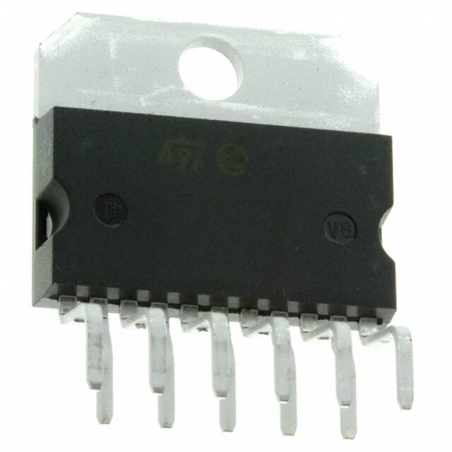
MULTIWATT11
(In line)
PowerSO-20
Description
The L6370 is a monolithic Intelligent Power
Switch in Multipower BCD Technology, for driving
inductive or resistive loads. An internal Clamping
Diode enables the fast demagnetization of
inductive loads. Diagnostic for CPU feedback and
extensive use of electrical protections make this
device extremely rugged and specially suitable for
industrial automation applications..
Table 1. Device summary
Part number
Op. Temp. range, °C
Package
Packaging
L6370L
-25 to +85
MULTIWATT11
Tube
L6370D
-25 to +85
PowerSO-20
Tube
L6370D013TR
-25 to +85
PowerSO-20
Tape & Reel
February 2007
Rev 6
1/20
www.st.com
20
�Contents
L6370
Contents
1
Block diagram and pin description . . . . . . . . . . . . . . . . . . . . . . . . . . . . . 3
1.1
2
3
4
5
2/20
Pin description . . . . . . . . . . . . . . . . . . . . . . . . . . . . . . . . . . . . . . . . . . . . . . 4
Electrical specifications . . . . . . . . . . . . . . . . . . . . . . . . . . . . . . . . . . . . . . 5
2.1
Absolute maximum ratings . . . . . . . . . . . . . . . . . . . . . . . . . . . . . . . . . . . . . 5
2.2
Thermal data . . . . . . . . . . . . . . . . . . . . . . . . . . . . . . . . . . . . . . . . . . . . . . . 5
2.3
Electrical characteristics . . . . . . . . . . . . . . . . . . . . . . . . . . . . . . . . . . . . . . . 6
2.4
AC operation . . . . . . . . . . . . . . . . . . . . . . . . . . . . . . . . . . . . . . . . . . . . . . . 8
Circuit description . . . . . . . . . . . . . . . . . . . . . . . . . . . . . . . . . . . . . . . . . . . 9
3.1
Diagnostic truth table . . . . . . . . . . . . . . . . . . . . . . . . . . . . . . . . . . . . . . . . 10
3.2
Input section . . . . . . . . . . . . . . . . . . . . . . . . . . . . . . . . . . . . . . . . . . . . . . . 10
3.3
Diagnostic logic . . . . . . . . . . . . . . . . . . . . . . . . . . . . . . . . . . . . . . . . . . . . 10
3.4
Short circuit operation . . . . . . . . . . . . . . . . . . . . . . . . . . . . . . . . . . . . . . . 11
3.5
Overtemperature protection (OVT) . . . . . . . . . . . . . . . . . . . . . . . . . . . . . . 11
3.6
Undervoltage protection (UV) . . . . . . . . . . . . . . . . . . . . . . . . . . . . . . . . . . 11
3.7
Demagnetization of inductive loads . . . . . . . . . . . . . . . . . . . . . . . . . . . . . 12
Package mechanical data . . . . . . . . . . . . . . . . . . . . . . . . . . . . . . . . . . . . 13
4.1
Multiwatt11 (in-line) mechanical data & package dimensions . . . . . . . . . 14
4.2
PowerSO-20 mechanical data & package dimensions . . . . . . . . . . . . . . . 15
4.3
PowerSO-20 packing information . . . . . . . . . . . . . . . . . . . . . . . . . . . . . . . 16
Revision history . . . . . . . . . . . . . . . . . . . . . . . . . . . . . . . . . . . . . . . . . . . 19
�L6370
1
Block diagram and pin description
Block diagram and pin description
Figure 1.
Block diagram
VS
UNDER
VOLTAGE
IN+
INPUT
IN-
CHARGE
PUMP
+
DRIVER
1.4V
OUT
NON DISSIPATIVE
SHORT CIRCUIT
ON-DELAY
CURRENT
LIMITATION
RSC
OPEN LOAD
DETECTION
OSC
OUTSTATUS
DIAG1
DIAGNOSTIC
THERMAL
PROTECTION
DIAG2
3mA
OUTPUT STATUS
Figure 2.
D95IN208D
Pin connection (top view)
11
OUTPUT
10
SUPPLY VOLTAGE
9
OUTPUT
8
RSC
7
ON-DELAY
6
GND
5
OUTPUT STATUS
4
INPUT -
3
INPUT +
2
DIAGNOSTIC 2
1
DIAGNOSTIC 1
MULTIWATT11
D95IN209A
GND
1
20
GND
OUTPUT
2
19
OUTPUT STATUS
OUTPUT
3
18
INPUT -
ON-DELAY
4
17
INPUT +
SUPPLY VOLTAGE
5
16
N.C.
SUPPLY VOLTAGE
6
15
DIAGNOSTIC 2
DIAGNOSTIC 1
N.C.
7
14
OUTPUT
8
13
RSC
OUTPUT
9
12
N.C.
10
11
GND
PowerSO-20
GND
D95IN210B
Note: Output pins must be connected externally to the package to use all leads for the output
current (Pin 9 and 11 for Multiwatt package, Pin 2, 3, 8 and 9 for PowerSO20 package).
3/20
�Block diagram and pin description
1.1
Pin description
Table 2.
4/20
L6370
Pin description (pin numbering referred to MULTIWATT package)
Pin N°
Pin name
1
DIAG1
DIAGNOSTIC 1 output. This open drain reports the IC working
conditions. (See Diagnostic truth Table 7)
2
DIAG2
DIAGNOSTIC 2 output. This open drain reports the IC working
conditions. (See Diagnostic truth Table 7)
3
IN-
Comparator non inverting input
4
IN+
Comparator inverting input
5
OUTSTATUS
6
GND
7
ON-DELAY
8
RSC
9
OUTPUT
10
VS
11
OUTPUT
Function
This current source output is capable of driving a LED to signal the
status of the output pin. The pin is active (source current) when the
output pin is considered high (See Figure 3)
Ground
Programmable ON time interval duration during short circuit operation
Current limitation setting.
High Side output with built-in current limitation
Supply Volatge Input, the value of the supply voltage is monitored to
detect under voltage condition
High Side output with built-in current limitation
�L6370
Electrical specifications
2
Electrical specifications
2.1
Absolute maximum ratings
Table 3.
Absolute maximum ratings
(Pin numbering referred to MULTIWATT package)
Symbol
Value
Unit
VS
Supply Voltage (Pin 10) (TW< 10ms)
50
V
VS– VO
Supply to Output Differential Voltage.
See also VCl (Pins 10 - 9)
internally limited
V
Vod
Externally Forced Voltage (Pin7)
-0.3 to 7
V
Iod
Externally Forced Voltage (Pin7)
+1
mA
Vi
Input Voltage (Pins 3/4)
-10 to VS+10
V
Vi
Differential Input Voltage (Pins 3 - 4)
43
V
Ii
Input Current (Pins 3/4)
20
mA
IO
Output Current (Pin 9). See also ISC (Pin 9)
internally limited
A
PTOT
Power Dissipation.
See also Thermal Characteristics.
internally limited
W
TOP
Operating Temperature Range (Tamb)
-25 to +85
°C
TSTG
Storage Temperature
-55 to 150
°C
1
J
EI
2.2
Parameter
Energy Induct. Load TJ= 85°C
Thermal data
Table 4.
Symbol
Thermal data
Description
MULTIWATT11 PowerSO-20
RthJC
Thermal Resistance Junction to case
Max.
1.5
1.5
RthJA
Thermal Resistance Junction to ambient Max.
35
-
Unit
°C/W
5/20
�Electrical specifications
L6370
2.3
Electrical characteristics
Table 5.
Electrical characteristics
(VS = 24V; TJ = –25 to +125°C, unless otherwise specified)
Symbol
Vsmin
Parameter
Supply Voltage for Valid
Diagnostics
Test condition
Min.
Idiag> 0.5mA ; Vdg1= 1.5V
Typ.
Max.
Unit
35
V
24
35
V
0.8
3
1.4
4
mA
8.5
9
9.5
V
4
Vs
Supply Voltage (operative)
Iq
Quiescent Current
Iout = Ios = 0
Vil
Vih
Vsth1
Undervoltage Threshold 1
(See Figure 3), Tamb = 0 to
+85°C
Vsth2
Undervoltage Threshold 2
8
8.5
9
V
Vsth3
Supply Voltage Hysteresis
300
500
700
mV
Isc
Short Circuit Current
9.5
VS = 9.5 to 35V; RL= 2Ω 5kΩ<
RSC< 30kΩ
0< RSC< 5kΩ
Vdon
15/RSC(kΩ)
2.6
A
3.2
4
A
Iout = 2.0A
Tj = 25°C
Tj = 25°C
200
320
280
440
mV
Iout = 2.5A
Tj = 25°C
Tj = 25°C
250
400
350
550
mV
500
µA
0.8
1.5
V
Output Voltage Drop
Ioslk
Output Leakage Current
Vi = Vil; Vo = 0V
Vol
Low State Out Voltage
Vi = Vil; RL = ∞
Vcl
Internal Voltage Clamp
(VS- VO)
IO = 1A
Single Pulsed: Tp = 300µs
48
53
58
V
Iold
Open Load Detection Current
Vi = Vih; Tamb = 0 to +85°C
1
3
6
mA
Vid
Common Mode Input Voltage
Range (Operative)
VS = 18 to 35V
-7
15
V
Iib
Input Bias Current
Vi = -7 to 15V; -In = 0V
-250
250
µA
Vith
Input Threshold Voltage
V +In > V -In
0.8
2
V
Viths
Input Threshold Hysteresis
Voltage
V +In > V -In
50
400
mV
Rid
Diff. Input Resistance
0 < +In < +16V ; -In = 0V
-7 < +In < 0V ; -In = 0V
Iilk
6/20
Input Offset Current
1.4
400
150
V +In = V -In
0V < Vi < 5.5V
+Ii
-Ii
-20
-75
-25
-In = GND
0V < V+In V-In)
7/20
�Electrical specifications
L6370
2.4
AC operation
Table 6.
AC operation
(pin numbering referred to MULTIWATT package)
Symbol
Pin
Parameter
tr - tf
9 vs 4
Rise or Fall Time
td
9 vs 3
Delay Time
dV/dt
9, 11
Slew Rate (Rise and Fall Edge)
tON
7
On time during Short Circuit
Condition
Test condition
Min.
VS = 24V; RI = 70Ω;
Rl to ground
0.7
50pF < CDON < 2nF
Typ.
Max.
Unit
20
µs
5
µs
1
1.5
V/µs
1.28
µs/pF
tOFF
Of time during hort Circuit
Condition
64
tON
fmax
Maximum Operating
Frequency
25
KHz
8/20
�L6370
3
Circuit description
Circuit description
Figure 3.
Output status hysteresis
Vshys
Voth2
Figure 4.
Voth1
D95IN211A
VOUT
Undervoltage comparator hysteresis
Vshys
Voth1
Figure 5.
Voth2
D95IN212
Vs
Switching waveforms
Vin
50%
50%
td
t
td
Vout
90%
90%
50%
50%
10%
10%
tr
tf
D94IN127A
t
9/20
�Circuit description
3.1
L6370
Diagnostic truth table
Table 7.
Diagnostic truth table
Diagnostic conditions
Input
Output
Diag1
Diag2
Normal Operation
L
H
L
H
H
H
H
H
Open Load Condition (Io< Iold)
L
H
L
H
H
L
H
H
Short to VS
L
H
H
H
L
L
H
H
Short Circuit to Ground (IO = ISC) (**)
(pin ON-DELAY grounded)
H
H (*)
L
H
H
H
H
Output DMOS Open
L
H
L
L
H
L
H
H
Overtemperature
L
H
L
L
H
H
L
L
Supply Undervoltage (VS< Vsth2)
L
H
L
L
L
L
L
L
Note:
(*) According to the intervention of the current limiting block.
(**) A cold lamp filament, or a capacitive load may activate the current limiting circuit of the
IPS, when the IPS is initially turned on.
3.2
Input section
The input section is an high impedance differential stage with high common and differential
mode range. There’s built-in offset of +1.4V (typical value) and an hysteresis of 400mV
(maximum value), to ensure high noise immunity.
3.3
Diagnostic logic
The operating conditions of the device are permanently monitored and the following
occurences are signalled via the DIAG1/DIAG2 open-drain output pins:
10/20
–
Short Circuit versus ground. A current limiting circuit fixes at Isc = 3.2A (typical
value) the maximum current that can be sourced from the OUTPUT pin (for more
details see short circuit operation section).
–
Short Circuit versus Vs.
–
Under Voltage(UV)
–
Over Temperature (OVT)
–
Open Load, if the output current is less than 3mA (typical value).
–
Output DMOS Open according to the diagnostic Truth Table 7
�L6370
3.4
Circuit description
Short circuit operation
In order to minimise the power dissipation when the output is shorted to grounded, an
innovative, non dissipative short cicuit protection (patent pending) is implemented, avoiding,
thus the intervention of the thermal protection in most cases.
Whenever the output is shorted to ground, or, generally speaking, an over current is sinked
by the load, the output devices is driven in linear mode, sourcing the Isc current (typically
3.2A) for a time interval (ton) defined by means of the external CON capacitor connected
between the ONDELAY pin and GND. Whether the short circuit crease within the ton interval
the DIAG2 output status is not affected, acting as a Programmable Diagnostic Delay.
This function allow the device to drive a capacitive load or a filament lamp (that exhibits a
very low resistance during the initial heading phase) without the intervention of the
diagnostic. If the short circuit lasts for the whole tON interval, the output DMOS is switched
OFF and the DIAG2 goes low, for a time interval tOFF lasting 64 times tON.
At the end of the tOFF interval if the short circuit condition is still present, the output DMOS is
turned ON (and the DIAG2 goes high - see Figure 7) for another tON interval and the
sequence starts again, or, whether not, the normal condition operation is resumed.
The tON interval can be set to lasts between 64ms and 2.56ms for a CON capacitor value
ranging between 50pF and 2nF to have:
tON (µs) = 1.28 CON (pF)
If the ON-DELAY pin is grounded the non dissipative short circuit protection is disabled, and
the Isc current is delivered until the Overtemperature Protection shuts the device off. The
behaviour of the DIAG2 output is, in this situation, showed in the Diagnostic Truth Table 7.
3.5
Overtemperature protection (OVT)
If the chip temperature exceeds Qlim (measured in a central position in the chip) the chip
deactivates itself.
The following actions are taken:
all the output stage is switched off;
the signal DIAG2 is activated (active low).
Normal operation is resumed as soon as (typically after some seconds) the chip
temperature monitored goes back below Θlim-ΘH.
The different thresholds with hysteretic behavior assure that no intermittent conditions can
be generated.
3.6
Undervoltage protection (UV)
The supply voltage is expected to range from 9.5V to 35V, even if its reference value is
considered to be 24V.
In this range the device operates correctly. Below 9.5V the overall system has to be
considered not reliable.
Protection will thus shut off the output whenever the supply voltage falls below the mask
fixed by the Vsth1(9V typ.) and Vsth2 (8.5V typ.).
11/20
�Circuit description
L6370
The hysteresis (see Figure 4) ensures a non intermittent behavior at low supply voltage with
a superimposed ripple. The Under Voltage status is signalled via the DIAG1 and DIAG2
outputs (see the Diagnostic Truth Table 7) .
3.7
Demagnetization of inductive loads
An internal zener diode, limiting the voltage across the Power MOS to between 50 and 60V
(Vcl), provides safe and fast demagnetization of inductive loads without external clamping
devices. The maximum energy that can be absorbed from an inductive load is specified as
1J (at Tj = 85°C) (see Figure 4).
Figure 6.
L6370 short circuit operation waveforms
Figure 7.
Inductive load equivalent circuit
+VS
IS
50V
VS
OUTPUT
IO
RL
D95IN215A
12/20
L
�L6370
4
Package mechanical data
Package mechanical data
In order to meet environmental requirements, ST offers these devices in ECOPACK®
packages. These packages have a Lead-free second level interconnect . The category of
second level interconnect is marked on the package and on the inner box label, in
compliance with JEDEC Standard JESD97. The maximum ratings related to soldering
conditions are also marked on the inner box label. ECOPACK is an ST trademark.
ECOPACK specifications are available at: www.st.com
13/20
�Package mechanical data
4.1
L6370
MULTIWATT11 (in-line) mechanical data & package
dimensions
Figure 8.
MULTIWATT11 (in-line) mechanical data & package dimensions
mm
inch
DIM.
MIN.
TYP.
MAX.
MIN.
TYP.
MAX.
A
5
0.197
B
2.65
0.104
C
1.6
0.063
E
0.49
0.55
0.019
0.022
F
0.88
0.95
0.035
0.037
G
1.57
1.7
1.83
0.062
0.067
0.072
G1
16.87
17
17.13
0.664
0.669
0.674
H1
19.6
0.772
H2
L
OUTLINE AND
MECHANICAL DATA
20.2
26.4
26.9
0.795
1.039
1.059
L1
22.35
22.85
0.880
L3
17.25
17.5
17.75
0.679
0.689
0.699
0.900
L4
10.3
10.7
10.9
0.406
0.421
0.429
L7
2.65
2.9
0.104
0.114
S
1.9
2.6
0.075
0.102
S1
1.9
2.6
0.075
0.102
Dia1
3.65
3.85
0.144
0.152
MULTIWATT11
Multiwatt11
(In-Line)
0016039 F
14/20
�L6370
4.2
Package mechanical data
PowerSO-20 mechanical data & package dimensions
Figure 9.
DIM.
PowerSO-20 mechanical data & package dimensions
mm
MIN.
TYP.
A
a1
inch
MAX.
MIN.
TYP.
3.6
0.1
0.3
a2
0.142
0.004
0.012
3.3
0.130
a3
0
0.1
0.000
0.004
b
0.4
0.53
0.016
0.021
c
0.23
0.32
0.009
0.013
D (1)
15.8
16
0.622
0.630
D1 (2)
9.4
9.8
0.370
0.386
E
13.9
14.5
0.547
e
1.27
e3
E1 (1)
E3
0.570
0.450
11.1
E2
0.429
0.437
0.228
0.244
2.9
5.8
6.2
0.114
G
0
0.1
0.000
0.004
H
15.5
15.9
0.610
0.626
0.8
1.1
0.031
0.043
h
L
1.1
0.043
N
8˚(typ.)
S
8˚(max. )
T
Weight: 1.9gr
0.050
11.43
10.9
OUTLINE AND
MECHANICAL DATA
MAX.
10
JEDEC MO-166
0.394
PowerSO-20
(1) “D and E1” do not include mold flash or protusions.
- Mold flash or protusions shall not exceed 0.15mm (0.006”)
- Critical dimensions: “E”, “G” and “a3”.
(2) For subcontractors, the limit is the one quoted in jedec MO-166
N
R
N
a2
b
A
e
DETAIL A
c
a1
DETAIL B
E
e3
H
DETAIL A
lead
D
slug
a3
DETAIL B
20
11
0.35
Gage Plane
-C-
S
SEATING PLANE
L
G
E2
E1
BOTTOM VIEW
C
(COPLANARITY)
T
E3
1
h x 45˚
1
0
PSO20MEC
D1
0056635 I
15/20
�Package mechanical data
4.3
L6370
PowerSO-20 packing information
Figure 10. PowerSO-20 tube shipment information
TUBE MECHANICAL DATA
A
16/20
mm.
inch
18.80
0.740
B
17.2 ±0.2
0.677 ±0.008
C
8.20 ±0.2
0.323 ±0.008
D
10.90 ±0.2
0.429 ±0.008
E
2.90 ±0.2
0.114 ±0.008
F
0.40
0.016
G
0.80
0.031
H
6.30
0.248
I
4.30 ±0.2
0.165 ±0.008
J
3.7 ±0.2
0.146 ±0.008
K
9.4
0.370
L
0.40
0.016
M
0.80
0.031
N
3.50 ±0.2
0.138 ±0.008
BASE QUANTITY
31 pcs.
BULK QUANTITY
310 pcs.
�L6370
Package mechanical data
Figure 11. PowerSO-20 tape shipment specification
TAPE MECHANICAL DATA
D
mm.
inch
1.50 +0.1/0
0.059 +0.004/0
E
1.75 ±0.1
0.069 ±0.004
Po
4.00 ±0.1
0.157 ±0.004
T max.
0.40
0.016
D1 min.
1.50
0.059
0.453 ±0.002
F
11.5 ±0.05
K max.
6.50
0.256
P2
2.00 ±0.1
0.079 ±0.004
R
50
1.968
W
24.00 ±0.30
0.945 ±0.012
P1
24.00
0.945
Ao, Bo, Ko
0.05 min to 1.0 max.
0.002 min to 0.039 max.
BASE QUANTITY
600 pcs.
BULK QUANTITY
600 pcs.
17/20
�Package mechanical data
L6370
Figure 12. PowerSO-20 reel shipment specification
T
40mm (1.575in) min.
access hole
at slot location
B
C
D
A
N
G measured
at hub
Full radius
Tape slot in core for tape start
2.5mm (0.098in) min. width
REEL MECHANICAL DATA
mm.
inch
Tape size
24.0 ±0.30
0.945 ±0.012
A max.
330.0
12.992
B min.
1.5
0.059
C
13.0 ±0.20
0.512 ±0.008
D min.
20.2
0.795
N min.
60
2.362
G
24.4 +2/-0
0.960 +0.079/-0
T max.
30.4
1.197
Figure 13. Footprint recommended data
FOOTPRINT DATA
18/20
mm.
inch
A
9.5
0.374
B
14.7-15.0
0.579-0.591
C
12.5-12.7
0.492-0.500
D
6.3
0.248
E
0.64
0.026
F
0.71
0.028
G
1.27
0.050
�L6370
5
Revision history
Revision history
Table 8.
Revision history
Date
Revision
Changes
10-Aug-2003
3
Initial release.
12-Dec-2005
4
Applied new Look & Feel Style Sheet.
Added L6370D013TR part number.
Updated Package and Packing section.
26-Apr-2006
5
Document has been reformatted
19-Feb-2007
6
Typo in Figure 2 on page 3.
19/20
�Revision history
L6370
Please Read Carefully:
Information in this document is provided solely in connection with ST products. STMicroelectronics NV and its subsidiaries (“ST”) reserve the
right to make changes, corrections, modifications or improvements, to this document, and the products and services described herein at any
time, without notice.
All ST products are sold pursuant to ST’s terms and conditions of sale.
Purchasers are solely responsible for the choice, selection and use of the ST products and services described herein, and ST assumes no
liability whatsoever relating to the choice, selection or use of the ST products and services described herein.
No license, express or implied, by estoppel or otherwise, to any intellectual property rights is granted under this document. If any part of this
document refers to any third party products or services it shall not be deemed a license grant by ST for the use of such third party products
or services, or any intellectual property contained therein or considered as a warranty covering the use in any manner whatsoever of such
third party products or services or any intellectual property contained therein.
UNLESS OTHERWISE SET FORTH IN ST’S TERMS AND CONDITIONS OF SALE ST DISCLAIMS ANY EXPRESS OR IMPLIED
WARRANTY WITH RESPECT TO THE USE AND/OR SALE OF ST PRODUCTS INCLUDING WITHOUT LIMITATION IMPLIED
WARRANTIES OF MERCHANTABILITY, FITNESS FOR A PARTICULAR PURPOSE (AND THEIR EQUIVALENTS UNDER THE LAWS
OF ANY JURISDICTION), OR INFRINGEMENT OF ANY PATENT, COPYRIGHT OR OTHER INTELLECTUAL PROPERTY RIGHT.
UNLESS EXPRESSLY APPROVED IN WRITING BY AN AUTHORIZED ST REPRESENTATIVE, ST PRODUCTS ARE NOT
RECOMMENDED, AUTHORIZED OR WARRANTED FOR USE IN MILITARY, AIR CRAFT, SPACE, LIFE SAVING, OR LIFE SUSTAINING
APPLICATIONS, NOR IN PRODUCTS OR SYSTEMS WHERE FAILURE OR MALFUNCTION MAY RESULT IN PERSONAL INJURY,
DEATH, OR SEVERE PROPERTY OR ENVIRONMENTAL DAMAGE. ST PRODUCTS WHICH ARE NOT SPECIFIED AS "AUTOMOTIVE
GRADE" MAY ONLY BE USED IN AUTOMOTIVE APPLICATIONS AT USER’S OWN RISK.
Resale of ST products with provisions different from the statements and/or technical features set forth in this document shall immediately void
any warranty granted by ST for the ST product or service described herein and shall not create or extend in any manner whatsoever, any
liability of ST.
ST and the ST logo are trademarks or registered trademarks of ST in various countries.
Information in this document supersedes and replaces all information previously supplied.
The ST logo is a registered trademark of STMicroelectronics. All other names are the property of their respective owners.
© 2007 STMicroelectronics - All rights reserved
STMicroelectronics group of companies
Australia - Belgium - Brazil - Canada - China - Czech Republic - Finland - France - Germany - Hong Kong - India - Israel - Italy - Japan Malaysia - Malta - Morocco - Singapore - Spain - Sweden - Switzerland - United Kingdom - United States of America
www.st.com
20/20
�