L6376
0.5 A high-side driver quad intelligent power switch
Features
■ ■ ■ ■ ■ ■ ■ ■ ■ ■ ■ ■ ■ ■
Multipower BCD technology 0.5 A four independent outputs 9.5 to 35 V supply voltage range Internal current limit Non-dissipative over-current protection Thermal shutdown Under voltage lockout with hysteresys Diagnostic output for under voltage, over temperature and over current External asynchronous reset input Presettable delay for overcurrent Diagnostic Open ground protection Immunity against burst transient (IEC 61000-4-4) ESD protection (human body model ± 2 kV) Block diagram
220nF 22nF VS VCP VC VP
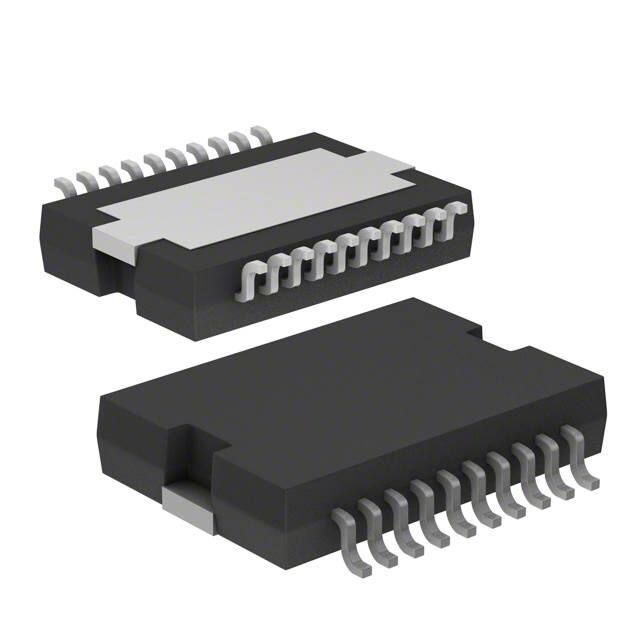
PowerSO-20
Description
This device is a monolithic quad intelligent power switch in multipower BCD technology, for driving inductive, capacitive or resistive loads. Diagnostic for CPU feedback and extensive use of electrical protections make this device inherently indistructible and suitable for general purpose industrial applications. Table 1. Device summary
Package PowerSO-20 PowerSO-20 Packaging Tube Tape and reel
Order codes L6376D L6376D013TR
Figure 1.
VS
CHARGE PUMP VCP
VS RS CURRENT LIMIT DRIVER OVC
GND
I1
+ -
O1 UV SHORT CIRCUIT CONTROL
I2
+ O2
I3
+ O3
I4
+ O4
R
+ OFF OSC 1.25V OFF DELAY CDOFF
DIAG
OVT
UV
ON OSC
ON DELAY CDON
D94IN076C
March 2008
Rev 6
1/18
www.st.com 18
�Contents
L6376
Contents
1 2 3 4 5 6 7 8 9 10 11 12 13 Maximum rating . . . . . . . . . . . . . . . . . . . . . . . . . . . . . . . . . . . . . . . . . . . . . 3 Pin connections . . . . . . . . . . . . . . . . . . . . . . . . . . . . . . . . . . . . . . . . . . . . . 4 Thermal characteristics . . . . . . . . . . . . . . . . . . . . . . . . . . . . . . . . . . . . . . 6 Electrical characteristics . . . . . . . . . . . . . . . . . . . . . . . . . . . . . . . . . . . . . 7 Overtemperature protection (OVT) . . . . . . . . . . . . . . . . . . . . . . . . . . . . 10 Undervoltage protection (UV) . . . . . . . . . . . . . . . . . . . . . . . . . . . . . . . . 10 Diagnostic logic . . . . . . . . . . . . . . . . . . . . . . . . . . . . . . . . . . . . . . . . . . . . 10 Short circuit operation . . . . . . . . . . . . . . . . . . . . . . . . . . . . . . . . . . . . . . 11 Programmable diagnostic delay . . . . . . . . . . . . . . . . . . . . . . . . . . . . . . 12 Reset input . . . . . . . . . . . . . . . . . . . . . . . . . . . . . . . . . . . . . . . . . . . . . . . . 12 Demagnetization of inductive loads . . . . . . . . . . . . . . . . . . . . . . . . . . . 13 Package mechanical data . . . . . . . . . . . . . . . . . . . . . . . . . . . . . . . . . . . . 15 Revision history . . . . . . . . . . . . . . . . . . . . . . . . . . . . . . . . . . . . . . . . . . . 17
2/18
�L6376
Maximum rating
1
Maximum rating
Table 2.
Symbol Vs Vs - Vout Vid Iid Ii Vi Iout Vout Eil Ptot Vdiag Idiag Top TJ Tstg 19 Externally forced current Ambient temperature, operating range Junction temperature, operating range (see overtemperature protection) Storage temperature -10 to 10 -25 to 85 -25 to 125 -55 to 150 mA °C °C °C 16, 17 Externally forced current 12, 13, Channel input current (forced) 14, 15, Channel input voltage 18 2, 3, 8, Output current (see also Isc) 9 Output voltage Energy inductive load (TJ =125 °C); each channel Power dissipation External voltage
Absolute maximum ratings
Pin 6 Parameter Supply voltage (tw ≤ 10 ms) Supply voltage (DC) Difference between supply voltage and output voltage Externally forced voltage Value 50 40 internally limited -0.3 to 7 ±1 ±2 -0.3 to 40 internally limited internally limited 200 internally limited -0.3 to Vs+0.7 V mJ V mA mA V Unit V V
3/18
�Pin connections
L6376
2
Pin connections
Figure 2. Pin connections (top view)
GND O4 O3 VP VC VS VCP O2 O1 GND
1 2 3 4 5 6 7 8 9 10
D95IN217
20 19 18 17 16 15 14 13 12 11
GND DIAG R OFF DELAY ON DELAY I4 I3 I2 I1 GND
Table 3.
N# 6
Pin description
Pin name VS Function Positive supply voltage. An internal circuit, monitoring the supply voltage, maintains the IC in OFF-state until VS reaches 9 V or when VS falls under 8.5 V. The diagnostic is availlable since VS = 5 V. Switch driver supply. To minimize the output drop voltage, a supply of about 10 V higher than VS is required. In order to use the built-in charge pump, connect a filter capacitor from pin1 to pin. The suggested value assures a fast transition and a low supply ripple even in worse condition. Using the four channels contemporarily, values less than 68 nF have to be avoided. High side outputs. Four independently controlled outputs with built-in current limitation. Ground and power dissipating pins. These pins are connected to the bulk ground of the IC, so are useful for heat dissipation.
7
VCP
2, 3, 8, 9 1, 10, 11, 20 12,13, 14, 15
O1, O2, O3, O4 GND
Control inputs. Four independent control signals. The output is held OFF I1, I2, I3, I4 until the voltage at the corresponding input pin reaches 1.35 V and is turned OFF when the voltage at the pin goes below 1.15 V. Programmable ON duration in short circuit. If an output is short circuited to ground or carryng a current exceeding the limit, the output is turned OFF and the diagnostic activation are delayed. This procedure allows the driving ON DELAY of hard surge current loads. The delay is programmed connecting a capacitor (50 pF to 15 nF) versus ground with the internal time constant of 1.28 µs/pF. The function can be disabled short circuiting this pin to ground. Programmable OFF duration in short circuit. After the short circuit or overcurrent detection, the switch is held OFF before the next attempt to switch on again. The delay is programmed connecting a capacitor (50 pF to 15 nF) versus ground with the internal time constant of 1.28 µs/pF. Short circuiting this pin to ground the OFF delay is 64 times the ON delay. Asyncronous reset input. This active low input (with hysteresis), switch off all the outputs independently from the input signal. By default it is biased low.
16
17
OFF DELAY
18
R
4/18
�L6376
Pin connections
Table 3.
N# 19
Pin description (continued)
Pin name DIAG Function Diagnostic output. This open drain output reports the IC working condition. The bad condition (as undervoltage, overcurrent, overtemperature) turns the output low. Pump oscillator voltage. At this pin is available the built-in circuitry to supply the switch driver at about 10 V higher than VS. To use this feature, connect a capacitor across pin 4 and pin 5. The suggested value assures a fast transition and a minimum output drop voltage even in worse condition. Using the four channels contemporarily, values less than 6.8 nF have to be avoided. Bootstrapped voltage. At this pin is available the 11 V oscillation for the charge pump, at a typical frequency of 200 kHz.
5
VC
4
VP
5/18
�Thermal characteristics
L6376
3
Thermal characteristics
Table 4.
Symbol RthJA RthJC
Thermal data
Parameter Thermal resistance, junction to ambient (see thermal characteristics) Thermal resistance junction-case Value 50 1.5 Unit °C/W °C/W
Note:
Additional data on the PowerSO-20 can be found in Application note AN668
6/18
�L6376
Electrical characteristics
4
Electrical characteristics
Table 5.
Symbol
Electrical characteristcs (Vs = 24 V; TJ = -25 to 125 °C; unless otherwise specified.)
Pin# Parameter Test condition Min Typ Max Unit
DC operation Vs Vsth Vshys Iqsc Vil Vih Ibias Vihys
Θlim ΘH
Supply voltage UV upperthreshold 6 UV hysteresis Quiescent current Input low level Input high level 12,13, 14,15, Input bias current 18 Input comparators hysteresis OVT upper threshold Threshold hysteresis Short circuit current Vs = 9.5 to 35 V; Rl = 2 Ω Iout = 500 mA; TJ = 25 °C Iout = 500 mA; TJ = 125 °C Outputs ON, no load
9.5 8.5 200
24 9 500 3
35 9.5 800 5 0.8 40
V V mV mA V V µA µA mV °C
0 2 Vi = 0 V Vi = 40 V -5 0 100 -1 5 200 150 20 0.65 0.9 320 460
0 20 400
30 1.2 500 640 100
°C A mV mV µA V V µA V µA
Isc
2, 3, 8, 9 Output voltage drop
Iolk Vcl Vol Idlkg 19 Vdiag Idch 16, 17
Output leakage current Internal voltage clamp (Vs-Vo each output) Low state output voltage
Vo = 0 V; Vi < 0.8 V Io = 100 mA single pulsed Tp = 300 µs Vi = Vil; RL = ∞ 47 52 0.8
57 1.5 25 1.5
Diagnostic output leakage Diagnostic off Diagnostic output voltage drop Delay capacitors charge current Idiag = 5 mA 40
7/18
�Electrical characteristics Table 5.
Symbol
L6376
Electrical characteristcs (continued) (Vs = 24 V; TJ = -25 to 125 °C; unless otherwise specified.)
Pin# Parameter Test condition Min Typ Max Unit
AC operation tr -tf 2, 3, 8, Rise or fall time 9 12 vs 9 13 vs 8 Delay time 14 vs 3 15 vs 2 2, 3, 8, Slew rate 9 (Rise and fall edge) On time during short circuit condition Off time during short circuit condition Maximum operating frequency Vs = 24 V; Rl = 47 Ω Rl to ground 3.8 µs
td
1
µs
dV/dt
Vs = 24 V; Rl = 47 Ω Rl to ground Rise Fall 50 pF < CDON < 15 nF pin 13 grounded 50 pF < CDOFF< 15 nF
3 4
5 7.6 1.28 64 1.28 25
7 10
V/µs V/µs µs/pF tON µs/pF kHz
tON
16
tOFF fmax
17
Source drain ndmos diode Vfsd Ifp trr tfr Forward on voltage Forward peak current Reverse recovery time Forward recovery time Ifsd = 500 mA tp = 10 ms; duty cycle = 20 % Ifsd = 500 mA; dIfsd/dt = 25 A/ms 200 50 1 1.5 1.5 V A ns ns
8/18
�L6376 Figure 3. Undervoltage comparator hysteresis
Electrical characteristics
Vshys
Vsth
D94IN126A
Vs
Figure 4.
Switching waveforms
Vin
50%
50%
td Vout 90% 50% 10% tr
td
t
90% 50% 10% tf
D94IN127A
t
9/18
�Overtemperature protection (OVT)
L6376
5
Overtemperature protection (OVT)
If the chip temperature exceeds Θlim (measured in a central position in the chip) the chip deactivates itself. The following actions are taken:
● ●
all the output stages are switched off; the signal DIAG is activated (active low).
Normal operation is resumed as soon as (typically after some seconds) the chip temperature monitored goes back below Θlim-ΘH. The different thresholds with hysteretic behavior assure that no intermittent conditions can be generated.
6
Undervoltage protection (UV)
The supply voltage is expected to range from 9.5 V to 35 V, even if its reference value is considered to be 24 V. In this range the device operates correctly. Below 9.5 V the overall system has to be considered not reliable. Consequently the supply voltage is monitored continuously and a signal, called UV, is internally generated and used. The signal is “on” as long as the supply voltage does not reach the upper internal threshold of the Vs comparator Vsth. The UV signal disappears above Vsth. Once the UV signal has been removed, the supply voltage must decrease below the lower threshold (i.e. Vsth-Vshys) before it is turned on again. The hysteresis Vshys is provided to prevent intermittent operation of the device at low supply voltages that may have a superimposed ripple around the average value. The UV signal switches off the outputs, but has no effect on the creation of the reference voltages for the internal comparators, nor on the continuous operation of the charge-pump circuits.
7
Diagnostic logic
The situations that are monitored and signalled with the DIAG output pin are:
●
current limit (OVC) in action; there are 4 individual current limiting circuits, one per each output; they limit the current that can be sunk from each output, to a typical value of 800 mA, equal for all of them; under voltage (UV); over temperature protection (OVT).
● ●
The diagnostic signal is transmitted via an open drain output (for ease of wired-or connection of several such signals) and a low level represents the presence of at least one of the monitored conditions, mentioned above.
10/18
�L6376
Short circuit operation
8
Short circuit operation
In order to allow normal operation of the other inputs when one channel is in short cirtuit, an innovative non dissipative over current protection (patent pending) is implemented in the device. Figure 5.
OUTPUT CURRENT Isc Iout
Short circuit operation waveforms
t


 工商网监
湘ICP备2023018690号
工商网监
湘ICP备2023018690号
