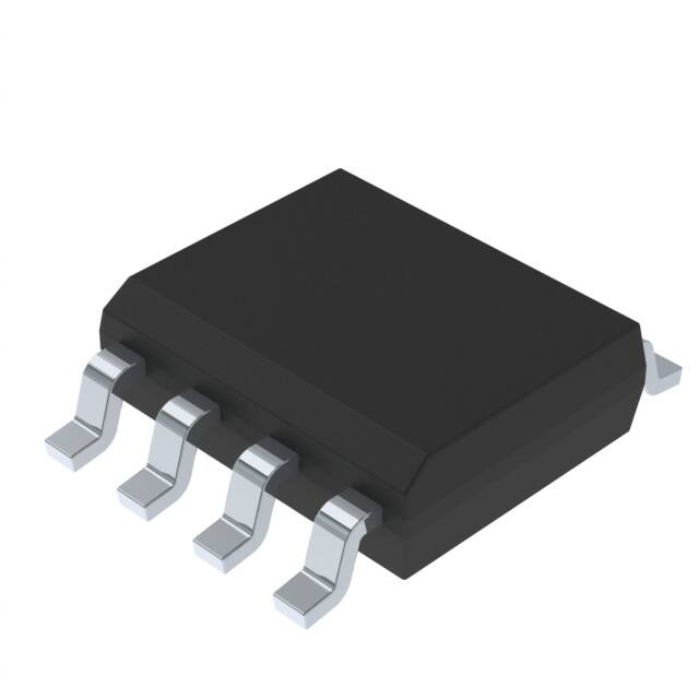
L6389E
High voltage high and low-side driver
Datasheet - production data
Description
SO-8
Features
High voltage rail up to 600 V
dV/dt immunity ± 50 V/nsec in full temperature
range
Driver current capability:
– 400 mA source
– 650 mA sink
Switching times 70/40 nsec rise/fall with 1 nF
load
3.3 V, 5 V, 15 V CMOS/TTL input comparators
with hysteresis and pull-down
Internal bootstrap diode
Outputs in phase with inputs
Deadtime and interlocking function
Applications
The L6389E is a high voltage gate driver,
manufactured with the BCD ™ “offline”
technology, and able to drive a half-bridge of
power MOSFET/IGBT devices. The high-side
(floating) section is enabled to work with voltage
rail up to 600 V. Both device outputs can sink and
source 650 mA and 400 mA respectively and
cannot be simultaneously driven high thanks to an
integrated interlocking function. Further
prevention from outputs cross conduction is
guaranteed by the deadtime function.
The L6389E device has two input and two output
pins, and guarantees the outputs switch in phase
with inputs. The logic inputs are CMOS/TTL
compatible (3.3 V, 5 V and 15 V) to ease the
interfacing with controlling devices.
The bootstrap diode is integrated in the driver
allowing a more compact and reliable solution.
The L6389E device features the UVLO protection
on both supply voltages (VCC and VBOOT)
ensuring greater protection against voltage drops
on the supply lines.
The device is available in an SO-8 tube, and tape
and reel packaging options.
Home appliances
Industrial applications and drives
Motor drivers
– DC, AC, PMDC and PMAC motors
Induction heating
HVAC
Factory automation
Lighting applications
Power supply systems
September 2016
This is information on a product in full production.
DocID029702 Rev 1
1/19
www.st.com
�Contents
L6389E
Contents
1
Block diagram . . . . . . . . . . . . . . . . . . . . . . . . . . . . . . . . . . . . . . . . . . . . . . 3
2
Electrical data . . . . . . . . . . . . . . . . . . . . . . . . . . . . . . . . . . . . . . . . . . . . . . 4
2.1
Absolute maximum ratings . . . . . . . . . . . . . . . . . . . . . . . . . . . . . . . . . . . . . 4
2.2
Thermal data . . . . . . . . . . . . . . . . . . . . . . . . . . . . . . . . . . . . . . . . . . . . . . . 4
2.3
Recommended operating conditions . . . . . . . . . . . . . . . . . . . . . . . . . . . . . 4
3
Pin connection . . . . . . . . . . . . . . . . . . . . . . . . . . . . . . . . . . . . . . . . . . . . . . 5
4
Electrical characteristics . . . . . . . . . . . . . . . . . . . . . . . . . . . . . . . . . . . . . 6
4.1
AC operation . . . . . . . . . . . . . . . . . . . . . . . . . . . . . . . . . . . . . . . . . . . . . . . 6
4.2
DC operation . . . . . . . . . . . . . . . . . . . . . . . . . . . . . . . . . . . . . . . . . . . . . . . 6
5
Waveform definitions . . . . . . . . . . . . . . . . . . . . . . . . . . . . . . . . . . . . . . . . 8
6
Input logic . . . . . . . . . . . . . . . . . . . . . . . . . . . . . . . . . . . . . . . . . . . . . . . . 10
7
Bootstrap driver . . . . . . . . . . . . . . . . . . . . . . . . . . . . . . . . . . . . . . . . . . . 10
CBOOT selection and charging . . . . . . . . . . . . . . . . . . . . . . . . . . . . . . . . . . . . . . . 10
8
Typical characteristics . . . . . . . . . . . . . . . . . . . . . . . . . . . . . . . . . . . . . . 13
9
Package information . . . . . . . . . . . . . . . . . . . . . . . . . . . . . . . . . . . . . . . . 15
9.1
SO-8 package information . . . . . . . . . . . . . . . . . . . . . . . . . . . . . . . . . . . . 15
10
Order codes . . . . . . . . . . . . . . . . . . . . . . . . . . . . . . . . . . . . . . . . . . . . . . . 17
11
Revision history . . . . . . . . . . . . . . . . . . . . . . . . . . . . . . . . . . . . . . . . . . . 18
2/19
DocID029702 Rev 1
�L6389E
Block diagram
1
Block diagram
Figure 1. Block diagram
#005453"1�%3*7&3
7$$
�
67
%&5&$5*0/
�
67
%&5&$5*0/
-0(*$
)*/
-*/
�
4)005
5)306()
13&7&/5*0/
)�7�
)7(
%3*7&3
3
3
-&7&4)*'5&3
7#005
$#005
)7(
�
4
065
7$$
�
-7(
%3*7&3
�
50�-0"%
�
-7(
�
(/%
".������
DocID029702 Rev 1
3/19
19
�Electrical data
L6389E
2
Electrical data
2.1
Absolute maximum ratings
Table 1. Absolute maximum ratings
Value
Symbol
Unit
Min.
Max.
VOUT
Output voltage
VBOOT -18
VBOOT
V
VCC
Supply voltage
- 0.3
18
V
Floating supply voltage
- 0.3
618
V
VBOOT
Vhvg
High-side gate output voltage
VOUT -0.3
VBOOT
V
Vlvg
Low-side gate output voltage
-0.3
VCC +0.3
V
Logic input voltage
-0.3
VCC +0.3
V
50
V/ns
Vi
dVOUT/dt
2.2
Parameter
Allowed output slew rate
Ptot
Total power dissipation (TA = 25 °C)
750
mW
TJ
Junction temperature
-45
150
°C
Ts
Storage temperature
-50
150
°C
ESD
Human body model
2
kV
Thermal data
Table 2. Thermal data
Symbol
Rth(JA)
2.3
Parameter
Thermal resistance junction to ambient
SO-8
Unit
150
°C/W
Recommended operating conditions
Table 3. Recommended operating conditions
Symbol
Pin
VOUT
6
VBS(2)
8
TJ
3
Test condition
Min.
Max.
Unit
(1)
580
V
Floating supply voltage
(1)
17
V
400
kHz
17
V
125
°C
HVG, LVG load CL = 1 nF
Supply voltage
Junction temperature
-45
1. If the condition VBOOT - VOUT < 18 V is guaranteed, VOUT can range from -3 to 580 V.
2. VBS = VBOOT - VOUT.
4/19
Typ.
Output voltage
Switching frequency
fsw
VCC
Parameter
DocID029702 Rev 1
�L6389E
3
Pin connection
Pin connection
Figure 2. Pin connection (top view)
Table 4. Pin description
No.
Pin
Type
Function
1
LIN
I
Low-side driver logic input
2
HIN
I
High-side driver logic input
3
VCC
P
Low-voltage power supply
4
GND
P
Ground
5
LVG(1)
O
Low-side driver output
6
OUT
P
High-side driver floating reference
7
HVG(1)
O
High-side driver output
8
VBOOT
P
Bootstrap supply voltage
1. The circuit guarantees 0.3 V maximum on the pin (at Isink = 10 mA). This allows the omission of the
“bleeder” resistor connected between the gate and the source of the external MOSFET normally used to
hold the pin low.
DocID029702 Rev 1
5/19
19
�Electrical characteristics
L6389E
4
Electrical characteristics
4.1
AC operation
Table 5. AC operation electrical characteristics (VCC = 15 V; TJ = 25 °C)
Symbol
ton
toff
Pin
Parameter
Test condition
High/low-side driver turn-on
1 vs. 5 propagation delay
2 vs. 7 High/low-side driver turn-off
propagation delay
Min.
Typ.
Max.
Unit
VOUT = 0 V
225
300
ns
VOUT = 0 V
160
220
ns
tr
5, 7
Rise time
CL = 1000 pF
70
100
ns
tf
5, 7
Fall time
CL = 1000 pF
40
80
ns
DT
5, 7
Deadtime
325
470
615
ns
Min.
Typ.
Max.
Unit
4.2
DC operation
Table 6. DC operation electrical characteristics
Symbol
Pin
Parameter
Test condition
Low supply voltage section
VCCth1
VCC UV turn-on threshold
9.1
9.6
10.1
V
VCCth2
VCC UV turn-off threshold
7.9
8.3
8.8
V
VCC UV hysteresis
0.9
VCChys
IQCCU
3
IQCC
Undervoltage quiescent supply
current
VCC 9 V
250
330
A
Quiescent current
VCC = 15 V
350
450
A
VCC 12.5 V
125
Bootstrap driver on
RDS(on)
V
resistance(1)
Bootstrapped supply voltage section
VBSth1
VBS UV turn-on threshold
8.5
9.5
10.5
V
VBSth2
VBS UV turn-off threshold
7.2
8.2
9.2
V
VBS UV hysteresis
0.9
VBShys
8
IQBS
VBS quiescent current
High voltage leakage current
ILK
V
HVG ON
250
A
Vhvg = VOUT = VBOOT = 600 V
10
A
High/low-side driver
Iso
Isi
6/19
5, 7
Source short-circuit current
VIN = Vih (tp < 10 s)
300
400
mA
Sink short-circuit current
VIN = Vil (tp < 10 s)
500
650
mA
DocID029702 Rev 1
�L6389E
Electrical characteristics
Table 6. DC operation electrical characteristics (continued)
Symbol
Pin
Parameter
Test condition
Min.
Typ.
Max.
Unit
1.1
V
Logic inputs
Vil
Vih
Iih
Iil
RP-DN
Low logic level input voltage
1, 2
High logic level input voltage
1.8
High logic level input current
VIN = 15 V
13
Low logic level input current
VIN = 0 V
-1
Logic inputs pull-down resistor
VIN = 15 V
600
V
20
25
A
A
750
1150
kΩ
1. RDS(on) is tested in the following way:
V CC – V BOOT1 – V CC – V BOOT2
R DSON = ----------------------------------------------------------------------------------------------I 1 V CC ,V BOOT1 – I 2 V CC ,V BOOT2
where:
I1 is pin 8 current when VBOOT = VBOOT1, I2 when VBOOT = VBOOT2.
DocID029702 Rev 1
7/19
19
�Waveform definitions
5
L6389E
Waveform definitions
Figure 3. Input to output waveform definition
���
���
��
��
��
��
��
��
��� ����
��
��� ����
��
����������
Figure 4. Propagation delay waveform definition
-*/
���
���
��%5
��%5
)*/
���
���
���
US
-7(
���
���
US
)7(
���
���
���
���
U PO
U PO
UG
UG
���
U PGG
���
U PGG
".������
8/19
DocID029702 Rev 1
�L6389E
Waveform definitions
Figure 5. Deadtime waveform definition
U���%5
-*/
)*/
���
���
���
���
UG
US
���
���
���
-7(
���
U PG G
UG
���
)7(
���
U PG G
���
%5 -)
%5 )".������
DocID029702 Rev 1
9/19
19
�Input logic
6
L6389E
Input logic
Table 7. Truth table
Input
Output
HIN
LIN
HVG
LVG
0
0
0
0
0
1
0
1
1
0
1
0
1
1
0
0
Input logic is provided with an interlocking circuitry which avoids the two outputs (LVG, HVG)
being active at the same time when both the logic input pins (LIN, HIN) are at a high logic
level. In addition, to prevent cross conduction of the external MOSFETs, after each output is
turned off, the other output cannot be turned on before a certain amount of time (DT) (see
Figure 3).
7
Bootstrap driver
A bootstrap circuitry is needed to supply the high voltage section. This function is normally
accomplished by a high voltage fast recovery diode (Figure 6 a). In the L6389E device,
a patented integrated structure replaces the external diode. It is realized by a high voltage
DMOS, driven synchronously with the low-side driver (LVG), with a diode in series, as
shown in Figure 6 b. An internal charge pump (Figure 6 b) provides the DMOS driving
voltage. The diode connected in series to the DMOS has been added to avoid an
undesirable turn-on.
CBOOT selection and charging
To choose the proper CBOOT value, the external MOSFET can be seen as an equivalent
capacitor. This capacitor CEXT is related to the MOSFET total gate charge:
Equation 1
Q gate
C EXT = --------------V gate
The ratio between the capacitors CEXT and CBOOT is proportional to the cyclical voltage loss.
It must be:
CBOOT>>>CEXT
E.g.: if Qgate is 30 nC and Vgate is 10 V, CEXT is 3 nF. With CBOOT = 100 nF the drop is
300 mV.
If HVG must be supplied for a long period, the CBOOT selection must also take the leakage
losses into account.
10/19
DocID029702 Rev 1
�L6389E
Bootstrap driver
E.g.: HVG steady-state consumption is typical 250 A, so, if HVG TON is 5 ms, CBOOT must
supply 1.25 C to CEXT. This charge on a 1 F capacitor means a voltage drop of 1.25 V.
The internal bootstrap driver offers important advantages: the external fast recovery diode
can be avoided (it usually has a high leakage current).
This structure can work only if VOUT is close to GND (or lower) and, at the same time, the
LVG is on. The charging time (Tcharge) of the CBOOT is the time in which both conditions are
fulfilled and it must be long enough to charge the capacitor.
The bootstrap driver introduces a voltage drop due to the DMOS RDS(on) (typical value:
125 ). This drop can be neglected at low switching frequency, but it should be taken into
account when operating at high switching frequency.
The following equation is useful to compute the drop on the bootstrap DMOS:
Equation 2
Q gate
V drop = I ch arg e R dson V drop = -------------------R dson
T ch arg e
where Qgate is the gate charge of the external power MOSFET, RDS(on) is the on-resistance
of the bootstrap DMOS, and Tcharge is the charging time of the bootstrap capacitor.
For example: using a power MOSFET with a total gate charge of 30 nC, the drop on the
bootstrap DMOS is about 1 V, if the Tcharge is 5 s.
In fact:
Equation 3
30nC
V drop = --------------- 125 0.8V
5s
Vdrop should be taken into account when the voltage drop on CBOOT is calculated: if this drop
is too high, or the circuit topology doesn’t allow a sufficient charging time, an external diode
can be used.
DocID029702 Rev 1
11/19
19
�Bootstrap driver
L6389E
Figure 6. Bootstrap driver
%#005
74
7#005
)�7�
)7(
$#005
7065
50�-0"%
-7(
B
7#005
74
)�7�
)7(
$#005
7065
50�-0"%
-7(
C
".������
12/19
DocID029702 Rev 1
�L6389E
Typical characteristics
8
Typical characteristics
Figure 7. Typical rise and fall times
vs. load capacitance
Figure 8. Quiescent current vs. supply voltage
UJNF
OTFD
���
���
���
���
5S
���
5G
���
���
��
��
�
�
�
�
�
�
�
$� O'
�
�
�
�
�
��
��
��
'PS�CPUI�IJHI�BOE�MPX�TJEF�CVGGFST�BU����$�5BNC
%��*/����
%��*/����W�
Figure 9. VBOOT UV turn-on threshold
vs. temperature
Figure 10. VCC UV turn-off threshold
vs. temperature
��
��
"U�7DD������7
��
��
5ZQ�
7DDUI�� 7
7#4UI�� 7
��
��
�� 74 7
�
�
�
�
5ZQ�
�
�
�
�
�
���
���
�
��
��
5K� $
��
���
���
".������
DocID029702 Rev 1
���
�
��
��
5K� $
��
��� ���
".������
13/19
19
�Typical characteristics
L6389E
Figure 11. VBOOT UV turn-off threshold
vs. temperature
Figure 12. Output source current
vs. temperature
����
��
���
$VSSFOU� N"
��
��
7#4UI �� 7
"U�7$$������7
"U�7$$������7
��
��
�
�
�
���
5ZQ�
���
���
5ZQ�
�
�
���
���
�
��
��
��
��� ���
���
���
�
".������
Figure 13. VCC UV turn-on threshold
vs. temperature
�� ��
5K� $
��
��� ���
".������
Figure 14. Output sink current
vs. temperature
��
����
"U�7$$������7
��
��
$VSSFOU� N"
7DDUI�� 7
���
��
�
5ZQ�
5ZQ�
���
���
�
�
�
���
14/19
���
���
�
��
��
5K� $
��
��� ���
���
".������
DocID029702 Rev 1
���
�
��
��
K�
5 $
��
��� ���
".������
�L6389E
9
Package information
Package information
In order to meet environmental requirements, ST offers these devices in different grades of
ECOPACK® packages, depending on their level of environmental compliance. ECOPACK
specifications, grade definitions and product status are available at: www.st.com.
ECOPACK is an ST trademark.
9.1
SO-8 package information
Figure 15. SO-8 package outline
$0�����Y�
DocID029702 Rev 1
15/19
19
�Package information
L6389E
Table 8. SO-8 package mechanical data
Dimensions (mm)
Symbol
Min.
Typ.
A
1.75
A1
0.10
0.25
A2
1.25
b
0.28
0.48
c
0.17
0.23
D
4.80
4.90
5.00
E
5.80
6.00
6.20
E1
3.80
3.90
4.00
e
1.27
h
0.25
0.50
L
0.40
1.27
L1
k
1.04
0°
8°
ccc
16/19
Max.
0.10
DocID029702 Rev 1
�L6389E
10
Order codes
Order codes
Table 9. Order codes
Part number
Package
Packaging
L6389ED
SO-8
Tube
L6389EDTR
SO-8
Tape and reel
DocID029702 Rev 1
17/19
19
�Revision history
11
L6389E
Revision history
Table 10. Document revision history
18/19
Date
Revision
08-Sep-2016
1
Changes
First release
DocID029702 Rev 1
�L6389E
IMPORTANT NOTICE – PLEASE READ CAREFULLY
STMicroelectronics NV and its subsidiaries (“ST”) reserve the right to make changes, corrections, enhancements, modifications, and
improvements to ST products and/or to this document at any time without notice. Purchasers should obtain the latest relevant information on
ST products before placing orders. ST products are sold pursuant to ST’s terms and conditions of sale in place at the time of order
acknowledgement.
Purchasers are solely responsible for the choice, selection, and use of ST products and ST assumes no liability for application assistance or
the design of Purchasers’ products.
No license, express or implied, to any intellectual property right is granted by ST herein.
Resale of ST products with provisions different from the information set forth herein shall void any warranty granted by ST for such product.
ST and the ST logo are trademarks of ST. All other product or service names are the property of their respective owners.
Information in this document supersedes and replaces information previously supplied in any prior versions of this document.
© 2016 STMicroelectronics – All rights reserved
DocID029702 Rev 1
19/19
19
�