L6451
28 channel inkjet driver
Features
■
Multipower BCD technology
■
40 V DMOS output breakdown
■
Precise output energy
■
ESD output protection with clamping diodes
■
Very low quiescent current
■
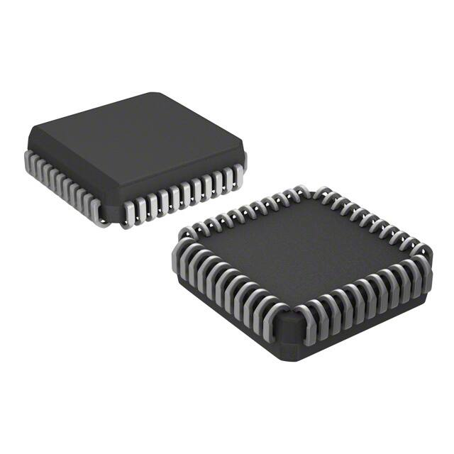
PLCC44 package
Description
The L6451 is realized in Multipower BCD
Technology which combines isolated DMOS
power transistors with CMOS and Bipolar circuits
on the same IC. By using mixed technology it has
been possible to optimize the logic circuitry and
the power stage to achieve the best possible
performances.
Table 1.
Device summary
Order codes
Package
L6451
PLCC44
L6451013TR
PLCC44 in tape and reel
L6451DIE8
DIE
Figure 1.
April 2009
PLCC44
Intended to be used in inkjet printer applications
as a 4 to 28 (2 x 14) line selectable
decoder/driver, the L6451 device driver has the
advantages of low power CMOS inputs and logic,
with 28 high current and high voltage DMOS
outputs capable of sustaining a maximum of 40 V.
On system power up the output drivers are locked
out using the chip enable function; two enable
inputs are available for the different driver banks.
An internal power-on system is implemented in
order to avoid wrong output commutation during
the supply voltage transients.
Using a mask option during manufacturing allows
a different decoding. Control of the energy
delivered to the print head is made by means of a
special circuitry. All driver outputs are capable of
withstanding a contact discharge of +/-8 kV with
the IC biased.
Block diagram (4-bit case)
Rev 4
1/9
www.st.com
9
�Pin information
L6451
1
Pin information
Figure 2.
Pin connection (top view)
Table 2.
Pin description
Pin Name
Function
VDD
5 V logic supply.
GND
Logic and power ground.
OUT0 to OUT27
DMOS outputs.
CLAMP
This pin has to be connected to the power supply voltage of the head resistors. Each of the
output DMOS have their drain connected with the anode of a protection diode, all the cathodes
of the protection diodes are connected to the clamp pin. In order to have the device supplied,
the CLAMP pin needs to be connected to the power.
INA, INB, INC, IND Decoder inputs.
COM1, COM2
A low logic input on these pins enables the outputs selected by the decoder inputs.
CHIP ENABLE
A logic high enable the chip.
2/9
�L6451
Electrical characteristics
2
Electrical characteristics
Table 3.
Absolute maximum ratings
Symbol
Parameter
Value
Unit
VOUT
Output voltage
40
V
VCLAMP
Output clamping voltage
40
V
IOUT
Output continuous current
0.8
A
IPEAK
Output peak current (with duty cycle = 10% TON= 4 ms)
2
A
TJ
Junction temperature
150
VDD
Logic supply voltage
7
V
VIN
Input voltage range
-0.3 V to VS+0.3
V
Tamb
Operating temperature range
Tstg
Storage temperature range
Table 4.
0 to 70
°C
-55 to 150
°C
Thermal data
Symbol
Rth j-amb
°C
Parameter
Value
Unit
65(1)
Thermal resistance junction-ambient max.
° C/W
1. Device mounted on PCB.
Table 5.
Symbol
DC electrical characteristcs(1)
Parameter
Test Condition
Min.
Typ.
Max.
Unit
4.75
5
5.25
V
38
V
1.2
V
VDD
Logic supply voltage
VCLAMP
Clamping voltage
VIL
Low level input voltage
VIH
High level input current
ILL
Low level input current
VIN= VIL
-200
μA
ILH
High level input current
VIN= VIH
10
μA
IDD
Logic supply current
(Independent from the output
conditions)
5
mA
VOUT
ΔVCE
Output saturation voltage
Output saturation absolute
voltage variation around the
typ. values for extended
temperature ranges
9
VDD -1.2
V
Tj = 25 ° C D.C. 0.4 A
0.9
V
Tj = 25 ° C D.C. 0.5 A
1.1
V
Tj = 90 ° C D.C. 0.4 A
1.4
V
Tj = 90 ° C D.C. 0.5 A
1.7
V
±0.2
±0.25
Tj = 25° C to 90° C D.C.: 0.4 A
Tj = 25° C to 90° C D.C.: 0.5 A
RDSON
2.2
V
V
Ω
1. Tamb = 25°C, VDD = 5V, Vclamp = 18 V unless otherwise specified
3/9
�Electrical characteristics
Table 6.
Symbol
L6451
AC electrical characteristics
Signal Name
Parameter
Test
Condition
Min.
Typ.
Max.
Unit
TS
INA, INB, INC,
IND Vs COMn
SET - UP time
30
ns
TH
INA, INB, INC,
IND Vs COMn
HOLD time
0
ns
Ton
COM1,2,3,4 VS OUT 0 to N
TURN - ON time
IOUT= 0.5 A,
RL= 39 Ω
Tj= 25 to
90 °C
Toff
COM1,2,3,4 VS OUT 0 to N
TURN - OFF time
IOUT= 0.5 A,
RL= 39 Ω
Tj= 25 to 90°C
150
ns
150
ns
tr
Rise time
100
ns
tf
Fall time
100
ns
Twout
Output pulse
width
ΔPD
Maximum
allowable variation
of the output
power transmitted
by each driver to
the resistive load
Figure 3.
4/9
Timing waveforms
Twin= 3.5 ms
RL= 40 Ω
IOUT= 0.5 A
-20
Twin
RL= 39 Ω
VCLAMP= 18 V
RL= 40 Ω
Vclamp= 18 V
±4
+80
ns
±4
%
%
�L6451
Functional description
3
Functional description
Table 7.
Decoder truth table
IND
INC
INB
INA (LSB)
OUTPUTS
0
0
0
0
0
0
0
0
1
1
1
1
1
1
1
1
0
0
0
0
1
1
1
1
0
0
0
0
1
1
1
1
0
0
1
1
0
0
1
1
0
0
1
1
0
0
1
1
0
1
0
1
0
1
0
1
0
1
0
1
0
1
0
1
0.27
1.26
2.25
3.24
4.23
5.22
6.21
7.20
8.19
9.18
10.17
11.16
12.15
13.14
ALL OFF
ALL OFF
Figure 4.
Application circuit
5/9
�Package information
4
L6451
Package information
In order to meet environmental requirements, ST offers these devices in different grades of
ECOPACK® packages, depending on their level of environmental compliance. ECOPACK®
specifications, grade definitions and product status are available at: www.st.com.
ECOPACK® is an ST trademark.
6/9
�L6451
Figure 5.
Package information
PLCC44 mechanical data and package dimensions
7/9
�Revision history
L6451
Revision history
Table 8.
8/9
Document revision history
Date
Revision
Description of Changes
Dec-2000
2
First Issue in EDOCS dms
May -2005
3
Changed only look and feel layout
02-Apr-2009
4
Converted to corporate template.
Added ECOPACK information.
�L6451
Please Read Carefully:
Information in this document is provided solely in connection with ST products. STMicroelectronics NV and its subsidiaries (“ST”) reserve the
right to make changes, corrections, modifications or improvements, to this document, and the products and services described herein at any
time, without notice.
All ST products are sold pursuant to ST’s terms and conditions of sale.
Purchasers are solely responsible for the choice, selection and use of the ST products and services described herein, and ST assumes no
liability whatsoever relating to the choice, selection or use of the ST products and services described herein.
No license, express or implied, by estoppel or otherwise, to any intellectual property rights is granted under this document. If any part of this
document refers to any third party products or services it shall not be deemed a license grant by ST for the use of such third party products
or services, or any intellectual property contained therein or considered as a warranty covering the use in any manner whatsoever of such
third party products or services or any intellectual property contained therein.
UNLESS OTHERWISE SET FORTH IN ST’S TERMS AND CONDITIONS OF SALE ST DISCLAIMS ANY EXPRESS OR IMPLIED
WARRANTY WITH RESPECT TO THE USE AND/OR SALE OF ST PRODUCTS INCLUDING WITHOUT LIMITATION IMPLIED
WARRANTIES OF MERCHANTABILITY, FITNESS FOR A PARTICULAR PURPOSE (AND THEIR EQUIVALENTS UNDER THE LAWS
OF ANY JURISDICTION), OR INFRINGEMENT OF ANY PATENT, COPYRIGHT OR OTHER INTELLECTUAL PROPERTY RIGHT.
UNLESS EXPRESSLY APPROVED IN WRITING BY AN AUTHORIZED ST REPRESENTATIVE, ST PRODUCTS ARE NOT
RECOMMENDED, AUTHORIZED OR WARRANTED FOR USE IN MILITARY, AIR CRAFT, SPACE, LIFE SAVING, OR LIFE SUSTAINING
APPLICATIONS, NOR IN PRODUCTS OR SYSTEMS WHERE FAILURE OR MALFUNCTION MAY RESULT IN PERSONAL INJURY,
DEATH, OR SEVERE PROPERTY OR ENVIRONMENTAL DAMAGE. ST PRODUCTS WHICH ARE NOT SPECIFIED AS "AUTOMOTIVE
GRADE" MAY ONLY BE USED IN AUTOMOTIVE APPLICATIONS AT USER’S OWN RISK.
Resale of ST products with provisions different from the statements and/or technical features set forth in this document shall immediately void
any warranty granted by ST for the ST product or service described herein and shall not create or extend in any manner whatsoever, any
liability of ST.
ST and the ST logo are trademarks or registered trademarks of ST in various countries.
Information in this document supersedes and replaces all information previously supplied.
The ST logo is a registered trademark of STMicroelectronics. All other names are the property of their respective owners.
© 2009 STMicroelectronics - All rights reserved
STMicroelectronics group of companies
Australia - Belgium - Brazil - Canada - China - Czech Republic - Finland - France - Germany - Hong Kong - India - Israel - Italy - Japan Malaysia - Malta - Morocco - Singapore - Spain - Sweden - Switzerland - United Kingdom - United States of America
www.st.com
9/9
�