L6722
3 Phase controller for DC/DC converters
Features
■
2A integrated gate drivers
■
0.8V reference
■
1% output voltage accuracy
■
Adjustable reference offset
)
s
(
t
c
u
Description
d
o
)
r
s
(
P
t
c
e
t
u
e
d
l
o
o
r
s
P
b
e
O
t
e
l
)
o
s
(
s
t
b
c
Applications
u
O
d
o
)
r
s
P
(
t
c
e
t
u
e
l
d
o
o
r
s
P
b
O
e
t
e
l
o
s
b
O
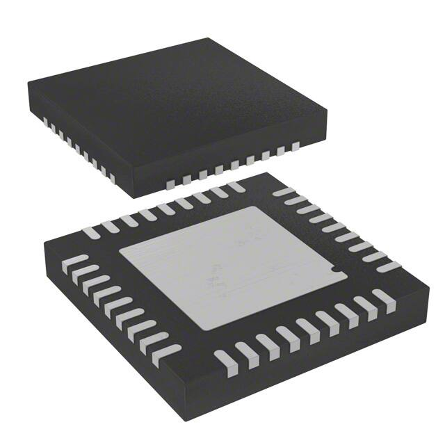
VFQFPN36
■
Precise current sharing and OCP across LS
MOSFETS
■
Constant over current protection
■
Feedback disconnection
■
LSLESS allows managing pre-bias startup
■
Preliminary of protection
■
Oscillator internally fixed at 100kHz, externally
adjustable
■
Power good
■
Integrated remote sense buffer
■
VFQFPN36 package with exposed pad
■
Memory supply for server and workstation MBs
■
High density DC / DC converters
■
High current pol
L6722 implements a three-phase step-down
controller with 120º phase-shift between each
phase with integrated high-current drivers in a
compact VFQFPN36 package with exposed pad.
L6722 manages output voltages down to 0.8V
with ±1% output voltage accuracy over line and
temperature variations. Additional programmable
offset can be added to the reference voltage with
a single external resistor in order to perform
margining tests.
The controller assures fast protection against load
over current and over / under voltage. In case of
over-current the system works in Constant
Current mode until UVP. Preliminary OVP allows
full load protection in case of startup with failed
HS. Feedback-disconnection protection prevents
from damaging the load in case of misconnections
in the remote sense. Pre-bias start-up is also
managed thanks to LSLESS.
Combined use of DCR and RdsON current
sensing assures precision in voltage positioning
(by reading droop current across inductors DCR)
and safe current sharing and OCP per each
phase (by reading the current across LS RdsON).
Droop function can be anyway disabled to
perform precise and load-insensitive regulation.
Order codes
May 2006
Part number
Package
Packing
L6722
VFQFPN36
Tube
L6722TR
VFQFPN36
Tape & Reel
Rev 1
1/34
www.st.com
34
�L6722
Contents
1
2
Typical application circuit and block diagram . . . . . . . . . . . . . . . . . . . . . . 4
1.1
Application circuit . . . . . . . . . . . . . . . . . . . . . . . . . . . . . . . . . . . . . . . . . . . . . . 4
1.2
Block diagram . . . . . . . . . . . . . . . . . . . . . . . . . . . . . . . . . . . . . . . . . . . . . . . . . 6
Pins description and connection diagrams . . . . . . . . . . . . . . . . . . . . . . . . 7
2.1
Pin description . . . . . . . . . . . . . . . . . . . . . . . . . . . . . . . . . . . . . . . . . . . . . . . . 7
)
s
(
t
c
u
d
o
)
r
s
(
P
t
c
e
t
u
e
d
l
o
o
r
s
P
b
e
O
t
e
l
)
o
s
(
s
t
b
c
u
O
d
o
)
r
s
P
(
t
c
e
t
u
e
l
d
o
o
r
s
P
b
O
e
t
e
l
o
s
b
O
2.2
3
Thermal data . . . . . . . . . . . . . . . . . . . . . . . . . . . . . . . . . . . . . . . . . . . . . . . . . 10
Electrical specifications . . . . . . . . . . . . . . . . . . . . . . . . . . . . . . . . . . . . . . . 11
3.1
Absolute maximum ratings . . . . . . . . . . . . . . . . . . . . . . . . . . . . . . . . . . . . . . 11
3.2
Electrical characteristics . . . . . . . . . . . . . . . . . . . . . . . . . . . . . . . . . . . . . . . . 11
4
Device description . . . . . . . . . . . . . . . . . . . . . . . . . . . . . . . . . . . . . . . . . . . . 13
5
Driver section . . . . . . . . . . . . . . . . . . . . . . . . . . . . . . . . . . . . . . . . . . . . . . . . 14
5.1
Power dissipation . . . . . . . . . . . . . . . . . . . . . . . . . . . . . . . . . . . . . . . . . . . . . 14
6
Current sharing loop and current reading . . . . . . . . . . . . . . . . . . . . . . . . 16
7
Output voltage positioning . . . . . . . . . . . . . . . . . . . . . . . . . . . . . . . . . . . . . 17
8
7.1
Offset and margining-mode (optional) . . . . . . . . . . . . . . . . . . . . . . . . . . . . . 17
7.2
Droop function (optional) . . . . . . . . . . . . . . . . . . . . . . . . . . . . . . . . . . . . . . . . 18
7.3
Maximum duty cycle limitation . . . . . . . . . . . . . . . . . . . . . . . . . . . . . . . . . . . 20
Soft start . . . . . . . . . . . . . . . . . . . . . . . . . . . . . . . . . . . . . . . . . . . . . . . . . . . . 21
8.1
9
2/34
Low-side-less startup for pre-bias output . . . . . . . . . . . . . . . . . . . . . . . . . . . 21
Output voltage monitor and protections . . . . . . . . . . . . . . . . . . . . . . . . . . 22
9.1
Under voltage . . . . . . . . . . . . . . . . . . . . . . . . . . . . . . . . . . . . . . . . . . . . . . . . 22
9.2
Over voltage . . . . . . . . . . . . . . . . . . . . . . . . . . . . . . . . . . . . . . . . . . . . . . . . . 22
9.3
Preliminary over voltage . . . . . . . . . . . . . . . . . . . . . . . . . . . . . . . . . . . . . . . . 22
9.4
Feedback disconnection . . . . . . . . . . . . . . . . . . . . . . . . . . . . . . . . . . . . . . . . 23
9.5
PGOOD . . . . . . . . . . . . . . . . . . . . . . . . . . . . . . . . . . . . . . . . . . . . . . . . . . . . . 24
�L6722
9.6
Over-current protection . . . . . . . . . . . . . . . . . . . . . . . . . . . . . . . . . . . . . . . . . 24
10
Oscillator . . . . . . . . . . . . . . . . . . . . . . . . . . . . . . . . . . . . . . . . . . . . . . . . . . . 26
11
System control loop compensation . . . . . . . . . . . . . . . . . . . . . . . . . . . . . . 27
11.1
12
Compensation network guidelines . . . . . . . . . . . . . . . . . . . . . . . . . . . . . . . . 28
Layout guidelines . . . . . . . . . . . . . . . . . . . . . . . . . . . . . . . . . . . . . . . . . . . . 30
12.1
Power components and connections . . . . . . . . . . . . . . . . . . . . . . . . . . . . . . 30
)
s
(
t
c
u
d
o
)
r
s
(
P
t
c
e
t
u
e
d
l
o
o
r
s
P
b
e
O
t
e
l
)
o
s
(
s
t
b
c
u
O
d
o
)
r
s
P
(
t
c
e
t
u
e
l
d
o
o
r
s
P
b
O
e
t
e
l
o
s
b
O
12.2
13
Small signal components and connections . . . . . . . . . . . . . . . . . . . . . . . . . . 30
Revision history . . . . . . . . . . . . . . . . . . . . . . . . . . . . . . . . . . . . . . . . . . . . . . 33
3/34
�L6722
1 Typical application circuit and block diagram
1
Typical application circuit and block diagram
1.1
Application circuit
Figure 1.
Typical application circuit
VIN
LIN
2
GNDIN
to BOOT1
to BOOT2
CIN
VCC
BOOT1
to BOOT3
7
8
)
s
(
t
c
u
d
o
)
r
s
(
P
t
c
e
t
u
e
d
l
o
o
r
s
P
b
e
O
t
e
l
)
o
s
(
s
t
b
c
u
O
d
o
)
r
s
P
(
t
c
e
t
u
e
l
d
o
o
r
s
P
b
O
e
t
e
l
o
s
b
O
4
1, 26
UGATE1
PGND
SGND
PHASE1
LGATE1
ROSC
18
OSC/INH/FLT
ISEN1
BOOT2
19
L6722
UGATE2
REF_IN
PHASE2
LGATE2
ISEN2
BOOT3
20
36
REF_OUT
COMP
PHASE3
CF
RF
UGATE3
35
LGATE3
FB
ISEN3
RFB
34
27
28
L6722 REFERENCE SCHEMATIC
4/34
CS+
VSEN
CS-
HS1
L1
9
3
31
LS1
RISEN
10
11
HS2
12
5
30
Vcc_core
L2
COUT
LS2
LOAD
RISEN
13
14
HS3
15
L3
6
29
LS3
RISEN
R1
32
R1
33
R2
R2
FBR
FBG
PGOOD
16
PGOOD
�L6722
1 Typical application circuit and block diagram
Figure 2.
Typical application circuit - droop enabled
VIN
LIN
2
GNDIN
4
1, 26
to BOOT1
VCC
BOOT1
UGATE1
PGND
SGND
PHASE1
LGATE1
ROSC
18
to BOOT2
CIN
OSC/INH/FLT
ISEN1
to BOOT3
7
8
HS1
L1
9
3
31
LS1
RISEN
)
s
(
t
c
u
d
o
)
r
s
(
P
t
c
e
t
u
e
d
l
o
o
r
s
P
b
e
O
t
e
l
)
o
s
(
s
t
b
c
u
O
d
o
)
r
s
P
(
t
c
e
t
u
e
l
d
o
o
r
s
P
b
O
e
t
e
l
o
s
b
O
LGATE2
ISEN2
BOOT3
20
36
REF_OUT
COMP
PHASE3
CF
RF
UGATE3
35
LGATE3
FB
ISEN3
RFB
34
CS+
VSEN
CS-
HS2
12
5
30
Vcc_core
L2
COUT
LS2
LOAD
RISEN
13
14
HS3
15
L3
6
29
LS3
RPH
REF_IN
PHASE2
11
RPH
19
L6722
UGATE2
10
RPH
BOOT2
RISEN
CPH
32
33
RD
27
28
FBR
FBG
PGOOD
16
PGOOD
L6722 REFERENCE SCHEMATIC - droop
5/34
�L6722
1 Typical application circuit and block diagram
VCC
VCC
PGND
PGND
VCC
LGATE3
PHASE3
UGATE3
BOOT3
LGATE2
PHASE2
UGATE2
BOOT2
LGATE1
PHASE1
Block diagram
BOOT1
Figure 3.
Block diagram
UGATE1
1.2
VCC
PGND
VCC
PGND
HS1
PGND
SGND
LS1
HS2
LOGIC PWM
ADAPTIVE ANTI
CROSS CONDUCTION
SGND
LS2
HS3
LOGIC PWM
ADAPTIVE ANTI
CROSS CONDUCTION
LS3
LOGIC PWM
ADAPTIVE ANTI
CROSS CONDUCTION
)
s
(
t
c
u
d
o
)
r
s
(
P
t
c
e
t
u
e
d
l
o
o
r
s
P
b
e
O
t
e
l
)
o
s
(
s
t
b
c
u
O
d
o
)
r
s
P
(
t
c
e
t
u
e
l
d
o
o
r
s
P
b
O
e
t
e
l
o
s
b
O
CURRENT SHARING
CORRECTION
PWM1
PWM2
PWM3
VCC
OCP1
L6722
CONTROL LOGIC
AND PROTECTIONS
OCP2
OCP3
LOW SIDE MOSFET
CURRENT READING
AND OVER CURRENT
OVP
FB
DISCONNECTION
IDROOP
VFB-DISC
SSEND / PGOOD
64k
IINFO
x3
64k
DROOP
CURRENT READING
REMOTE
BUFFER
VSEN
CS+
CS-
COMP
FB
REF_IN
ERROR
AMPLIFIER
REF_OUT
ISEN1
ISEN2
ISEN3
PGOOD
IOS
64k
64k
FBR
FBG
BANDGAP
AND REFERENCE
OSC/EN/FAULT
6/34
AVG
COMP
DIGITAL
SOFT START
PWM3
PH3
PWM2
PH2
PWM1
CURRENT SHARING
CORRECTION
PH1
OSC / INH / FLT
3 PHASE
OSCILLATOR
CURRENT SHARING
CORRECTION
�L6722
2
2 Pins description and connection diagrams
Pins description and connection diagrams
Pins connection (top view)
CSCS+
ISEN1
ISEN2
ISEN3
FBG
FBR
SGND
N.C.
Figure 4.
VSEN
FB
COMP
SGND
VCC
N.C.
LGATE1
PGND
LGATE2
36
35
34
33
1
32
31
30
29
28
27
2
26
3
25
4
24
5
23
6
22
7
21
8
20
N.C.
REF_OUT
REF_IN
N.C.
OSC / INH / FLT
N.C.
PGOOD
N.C.
PHASE3
)
s
(
t
c
u
d
o
)
r
s
(
P
t
c
e
t
u
e
d
l
o
o
r
s
P
b
e
O
t
e
l
)
o
s
(
2.1
Pin description
s
t
b
c
u
O
d
o
)
r
s
P
(
t
c
e
t
u
e
l
d
o
o
r
s
P
b
O
e
t
e
l
o
s
b
O
9
19
11
12
13
14
15
16
17
18
LGATE3
BOOT1
UGATE1
PHASE1
BOOT2
UGATE2
PHASE2
BOOT3
UGATE3
10
Table 1.
Pins description
Pin#
Name
Function
1
VSEN
2
FB
3
COMP
4
SGND
5
VCC
Device Power Supply as well as LS driver supply.
Operative voltage is 12V ±15%. Filter with at least 1µF MLCC vs. ground.
6
N.C.
Not Internally Bonded.
7
LGATE1
8
PGND
Remote Buffer Output. It manages OVP and UVP protections and
PGOOD. See Section 9 for details.
Error Amplifier Inverting Input. Connect with a resistor RFB vs. VSEN and
with an RF - CF vs. COMP.
Error Amplifier Output. Connect with an RF - CF vs. FB.
The device cannot be disabled by pulling down this pin.
All the internal references are referred to this pin. Connect to the PCB
Signal Ground.
Channel 1 LS Driver Output.
A small series resistor helps in reducing device-dissipated power.
LS Driver return path. Connect to Power ground Plane.
7/34
�L6722
2 Pins description and connection diagrams
Table 1.
Pins description (continued)
Pin#
Name
9
LGATE2
Channel 2 LS Driver Output.
A small series resistor helps in reducing device-dissipated power.
10
LGATE3
Channel 3 LS Driver Output.
A small series resistor helps in reducing device-dissipated power.
BOOT1
Channel 1 HS driver supply.
Connect through a capacitor (100nF typ.) to PHASE1 and provide
necessary Bootstrap diode.
A small series resistor before the boot diode helps in reducing Boot
capacitor overcharge.
11
Function
)
s
(
t
c
u
d
o
)
r
s
(
P
t
c
e
t
u
e
d
l
o
o
r
s
P
b
e
O
t
e
l
)
o
s
(
s
t
b
c
u
O
d
o
)
r
s
P
(
t
c
e
t
u
e
l
d
o
o
r
s
P
b
O
e
t
e
l
o
s
b
O
8/34
12
UGATE1
Channel 1 HS driver output.
A small series resistors helps in reducing device-dissipated power.
13
PHASE1
Channel 1 HS driver return path.
It must be connected to the HS1 mosfet source and provides return path
for the HS driver of channel 1.
14
BOOT2
Channel 2 HS driver supply.
Connect through a capacitor (100nF typ.) to PHASE2 and provide
necessary Bootstrap diode.
A small series resistor before the boot diode helps in reducing Boot
capacitor overcharge.
15
UGATE2
Channel 2 HS driver output.
A small series resistors helps in reducing device-dissipated power.
16
PHASE2
Channel 2 HS driver return path.
It must be connected to the HS2 mosfet source and provides return path
for the HS driver of channel 2.
17
BOOT3
Channel 3 HS driver supply.
Connect through a capacitor (100nF typ.) to PHASE3 and provide
necessary Bootstrap diode.
A small series resistor before the boot diode helps in reducing Boot
capacitor overcharge.
18
UGATE3
Channel 3 HS driver output.
A small series resistors helps in reducing device-dissipated power.
19
PHASE3
Channel 3 HS driver return path.
It must be connected to the HS3 mosfet source and provides return path
for the HS driver of channel 3.
20
N.C.
21
PGOOD
22
N.C.
Not Internally Bonded.
Open Drain Output set free after SS has finished and pulled low when
VSEN is lower than the relative threshold. Pull up to a voltage lower than
5V (typ), if not used it can be left floating.
Not Internally Bonded.
�L6722
2 Pins description and connection diagrams
Table 1.
Pin#
23
Pins description (continued)
Name
Function
OSC / INH /
FLT
Three functional pin:
OSC: It allows programming the switching frequency FSW of each
channel: the equivalent switching frequency at the load side results in
being tripled.
Frequency is programmed according to the resistor connected from the
pin vs. SGND or VCC with a gain of 4kHz/µA (see relevant section for
details). Leaving the pin floating programs a switching frequency of
100kHz per phase (300kHz on the load).
INH: Forced low, the device stops operations with all mosfets OFF: all the
protections are disabled except for Preliminary over voltage. It resets the
device from any latching condition.
FLT: The pin is forced high (5V) to signal an OVP FAULT: to recover from
this condition, cycle VCC or the OSC pin. See Section 10 for details.
)
s
(
t
c
u
d
o
)
r
s
(
P
t
c
e
t
u
e
d
l
o
o
r
s
P
b
e
O
t
e
l
)
o
s
(
s
t
b
c
u
O
d
o
)
r
s
P
(
t
c
e
t
u
e
l
d
o
o
r
s
P
b
O
e
t
e
l
o
s
b
O
24
N.C.
25
REF_IN
REFrence INput for the regulation. Connect directly or through a resistor
to the REF_OUT pin. See Section 7.1 for details.
26
REF_OUT
REFrence OUTput. Connect directly or through a resistor to the REF_IN
pin. See Section 7.1 for details.
27, 28
N.C.
29
SGND
30
FBR
Remote Buffer Non Inverting Input.
Connect to the positive side of the load to perform remote sense.
See Section 12 for proper layout of this connection.
31
FBG
Remote Buffer Inverting Input.
Connect to the negative side of the load to perform remote sense.
See Section 12 for proper layout of this connection.
32 to 34
ISEN3
to
ISEN1
LS Current Sense Pins.
These pins are used for current balance phase-to-phase as well as for the
system OCP. Connect through a resistor Rg to the relative PHASEx pin.
See Section 6 and Section 9.6 for details.
35
CS+
Droop Current Sense non-inverting input.
Connect through R-C network to the main inductors. See Section 7.1 for
details.
CS-
Droop Current Sense inverting input.
Connect through resistor RD to the main inductors common node. See
Section 7.1 for details.
This pin also monitor the feedback disconnection. See Section 9.4 for
details.
THERMAL
PAD
Thermal pad connects the Silicon substrate and makes good thermal
contact with the PCB to dissipate the power necessary to drive the
external mosfets.
Connect to the PGND plane with several VIAs to improve thermal
conductivity.
36
PAD
Not Internally Bonded.
Not Internally Bonded.
All the internal references are referred to this pin. Connect to the PCB
Signal Ground.
9/34
�L6722
2 Pins description and connection diagrams
2.2
Thermal data
Table 2.
Symbol
Thermal data
Parameter
Value
Unit
RthJA
Thermal Resistance Junction to Ambient
(Device soldered on 2s2p PC Board)
30
°C/W
TMAX
Maximum Junction Temperature
150
°C
TSTG
Storage Temperature Range
-40 to 150
°C
TJ
Junction Temperature Range
-40 to 125
°C
PTOT
Maximum Power Dissipation at TA = 25°C
)
s
(
t
c
u
d
o
)
r
s
(
P
t
c
e
t
u
e
d
l
o
o
r
s
P
b
e
O
t
e
l
)
o
s
(
s
t
b
c
u
O
d
o
)
r
s
P
(
t
c
e
t
u
e
l
d
o
o
r
s
P
b
O
e
t
e
l
o
s
b
O
10/34
3.5
W
�L6722
3 Electrical specifications
3
Electrical specifications
3.1
Absolute maximum ratings
Table 3.
Absolute maximum ratings
Symbol
VCC
VBOOTx - VPHASEx
Parameter
Value
Unit
to PGND
15
V
Boot Voltage
15
V
15
V
-0.3 to VCC + 0.3
V
-0.3 to 7
V
26
V
TBD
V
VUGATEx - VPHASEx
)
s
(
t
c
u
d
o
)
r
s
(
P
t
c
e
t
3.2
Electrical characteristics
u
e
d
l
o
o
r
s
P
b
e
O
t
e
l
)
o
s
(
s
t
b
c
u
O
d
o
)
r
s
P
(
t
c
e
t
u
e
l
d
o
o
r
s
P
b
O
e
t
e
l
o
s
b
O
LGATEx, PHASEx, to PGNDx
All other Pins to PGNDx
VPHASEx
Table 4.
Positive Peak Voltage; T
很抱歉,暂时无法提供与“L6722”相匹配的价格&库存,您可以联系我们找货
免费人工找货