L6756D
2/3/4 phase buck controller
for VR10, VR11 and VR11.1 processor applications
Features
■
LTB Technology® enhances load transient
response
■
2 to 4 scalable phase operation
■
Dual-edge asynchronous architecture
■
PSI# input with programmable strategy
■
Imon output
■
Flexible driver support
■
7/8 bit programmable output - VR10/11.1 DAC
■
0.5% output voltage accuracy
■
Full-differential current sense across DCR
■
Integrated remote sense buffer
■
Feedback disconnection protection
■
Adjustable oscillator from 100 kHz to 1 MHz
■
LSLess startup to manage pre-biased output
filter composition.
■
Programmable soft-start
■
Threshold sensitive enable pin for VTT
Sensing
■
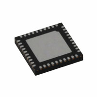
VFQFPN40 6x6 mm package
L6756D embeds selectable DAC: output voltage
is programmable up to 1.6000 V (Intel VR10 and
VR11.x DACs) managing DVID transitions with
±0.5% output voltage accuracy over line, load and
temperature variations.
VFQFPN40 6x6 mm
Description
L6756D is a two-to-four phase controller designed
to power Intel’s most demanding processors and,
most in general, low-voltage, high-current power
supplies. The device features LTB Technology® to
provide the fastest response to load transients
thus minimizing the output
The device assures fast protection against load
over current and under / over voltage. Feedback
disconnection prevents from damaging the load in
case of misconnections in the system board.
Applications
■
High-current VRM / VRD for desktop / server /
workstation CPUs
■
Graphic cards
■
Low-voltage, high-current power supplies
Low-side-less start-up allows soft-start over prebiased output avoiding dangerous current return
through the main inductors as well as negative
spike at the load side.
■
High-density DC / DC converters
L6756D is available in VFQFPN 6x6 mm package
Table 1.
Device summary
Order code
Package
Packing
L6756D
VFQFPN40
Tube
L6756DTR
VFQFPN40
Tape and reel
October 2008
Rev 1
1/36
www.st.com
1
�Contents
L6756D
Contents
1
2
3
Typical application circuit and block diagram . . . . . . . . . . . . . . . . . . . . 4
1.1
Application circuit . . . . . . . . . . . . . . . . . . . . . . . . . . . . . . . . . . . . . . . . . . . . 4
1.2
Block diagram . . . . . . . . . . . . . . . . . . . . . . . . . . . . . . . . . . . . . . . . . . . . . . . 7
Pins description and connection diagrams . . . . . . . . . . . . . . . . . . . . . . 8
2.1
Pin descriptions . . . . . . . . . . . . . . . . . . . . . . . . . . . . . . . . . . . . . . . . . . . . . 8
2.2
Thermal data . . . . . . . . . . . . . . . . . . . . . . . . . . . . . . . . . . . . . . . . . . . . . . 11
Electrical specifications . . . . . . . . . . . . . . . . . . . . . . . . . . . . . . . . . . . . . 12
3.1
Absolute maximum ratings . . . . . . . . . . . . . . . . . . . . . . . . . . . . . . . . . . . . 12
3.2
Electrical characteristics . . . . . . . . . . . . . . . . . . . . . . . . . . . . . . . . . . . . . . 12
4
Device description and operation . . . . . . . . . . . . . . . . . . . . . . . . . . . . . 19
5
Output voltage positioning . . . . . . . . . . . . . . . . . . . . . . . . . . . . . . . . . . . 20
5.1
Phase # programming . . . . . . . . . . . . . . . . . . . . . . . . . . . . . . . . . . . . . . . 20
5.2
Current reading and current sharing loop . . . . . . . . . . . . . . . . . . . . . . . . 21
5.3
Output voltage load-line definition . . . . . . . . . . . . . . . . . . . . . . . . . . . . . . 22
5.4
Output voltage offset . . . . . . . . . . . . . . . . . . . . . . . . . . . . . . . . . . . . . . . . 22
5.5
Dynamic VID transitions . . . . . . . . . . . . . . . . . . . . . . . . . . . . . . . . . . . . . . 23
5.6
Soft-start . . . . . . . . . . . . . . . . . . . . . . . . . . . . . . . . . . . . . . . . . . . . . . . . . . 24
5.6.1
6
LSLESS start-up . . . . . . . . . . . . . . . . . . . . . . . . . . . . . . . . . . . . . . . . . . 25
Output voltage monitoring and protections . . . . . . . . . . . . . . . . . . . . . 26
6.1
Overvoltage . . . . . . . . . . . . . . . . . . . . . . . . . . . . . . . . . . . . . . . . . . . . . . . 26
6.2
Feedback disconnection . . . . . . . . . . . . . . . . . . . . . . . . . . . . . . . . . . . . . . 26
6.3
VR_RDY . . . . . . . . . . . . . . . . . . . . . . . . . . . . . . . . . . . . . . . . . . . . . . . . . . 27
6.4
Over current . . . . . . . . . . . . . . . . . . . . . . . . . . . . . . . . . . . . . . . . . . . . . . . 27
7
Low power-state management and PSI# . . . . . . . . . . . . . . . . . . . . . . . . 28
8
Main oscillator . . . . . . . . . . . . . . . . . . . . . . . . . . . . . . . . . . . . . . . . . . . . . 29
2/36
�L6756D
9
Contents
System control loop compensation . . . . . . . . . . . . . . . . . . . . . . . . . . . 30
9.1
Compensation network guidelines . . . . . . . . . . . . . . . . . . . . . . . . . . . . . . 31
9.2
LTB Technology®
. . . . . . . . . . . . . . . . . . . . . . . . . . . . . . . . . . . . . . . . . . . . . . . . . . . . . . . 32
10
Mechanical data and package dimensions . . . . . . . . . . . . . . . . . . . . . . 34
11
Revision history . . . . . . . . . . . . . . . . . . . . . . . . . . . . . . . . . . . . . . . . . . . 35
3/36
�Typical application circuit and block diagram
L6756D
1
Typical application circuit and block diagram
1.1
Application circuit
Figure 1.
Typical 4phase application circuit
,).
6).
#$%#
�
#"5,+?).
6##
6##
'�
'�
� 6)$�
� 6)$�
'�
'�
� 6)$�
� 6)$�
$26/.
� 6)$�
� 6)$�
34,����$
62?2$9
�� 33
2/3#
�� 2/3#
2),)2,4"?'!).
�
��
�� ),)-
#3�
�
#(&
(3�
�
,�
,'!4%
'.$
�
2
,3�
��
#3�
#$%#
�
2'
6##
��
#3�. ��
#3�
2'
��
#3�. ��
"//4
2'
��
#3�. ��
2'
�
�
�
#&
62%& ��
#(
07-
%.
5'!4%
0(!3%
,'!4%
'.$
�
�
#(&
(3�
�
�
,�
2
,3�
03)?!�6)$?3%,
2&
��
2,4"
#,4"
#
&"'
63%.
��
)-/. ��
,4"
�� 6$20
�� 6&"
2&"
0(!3%
�
��
�� #/-0
2)
%.
5'!4%
��
#3�. ��
�� ,4"?'!).
#)
07-
��
�
#
#3�
�� 6)$�
�� 03)��62��
233
�
��
,����
06)$BUS)NTERFACINGWITH#05
� %.
� 6)$�
'.$
'.$
�
"//4
��
,����
�� ��
�� ��
#$%#
�
6##
"//4
�
�
07-
,����
�
%.
5'!4%
0(!3%
,'!4%
'.$
�
�
#(&
(3�
,�
�
�
2
,3�
#
#05
#-,##
#/54
#$%#
�
6##
�
�
�
07-
%.
'.$
,����
"//4
5'!4%
0(!3%
,'!4%
�
�
#(&
(3�
,�
�
�
,3�
2
#
!-�����V�
4/36
�L6756D
Typical application circuit and block diagram
Figure 2.
Typical 3phase application circuit
/,1
9,1
&'(&
�
&%8/.B,1
9&&
�9&&
�*�
�*�
� �9,'�
� �9,'�
�*�
�*�
� �9,'�
� �9,'�
'5921
� �9,'�
� �9,'�
�� 66
�� 526&
5,/,0
5/7%B*$,1
�
��
�
�� �,/,0
&6�
/�
�
/*$7(
�*1'
�
5
/6�
&6�
&'(&
�
5*
9&&
��
&6�1 ��
&6�
5*
��
�&6�1 ��
%227
5*
��
�&6�1 ��
5*
�
�
�
&)
95() ��
&+
�3:0
�(1
�*1'
8*$7(
3+$6(
/*$7(
�
�
&+)
+6�
�
�
/�
5
/6�
36,B$���9,'B6(/
5)
��
5/7%
&/7%
&
�)%*
�96(1
��
,021 ��
/7%
�� �9'53
�� �9)%
5)%
&+)
+6�
��
�� �&203
5,
3+$6(
�
��
&6�1 ��
�� �/7%B*$,1
&,
�(1
8*$7(
��
/����
67�/����'
�95B5'<
526&
�3:0
��
�
&
&6�
�� �9,'�
�� �36,����95��
566
�
��
�� ��
&'(&
�
9&&
%227
�
�
�
�3:0
�(1
�*1'
/����
39,'�EXV�,QWHUIDFLQJ�ZLWK�&38
� �(1
� �9,'�
�*1'
�*1'
�
%227
��
/����
�� ��
8*$7(
3+$6(
/*$7(
�
�
&+)
+6�
/�
�
�
/6�
5
&
&38
&0/&&
&287
!-�����V�
5/36
�Typical application circuit and block diagram
Figure 3.
L6756D
Typical 2phase application circuit
,).
6).
#$%#
�
#"5,+?).
6##
6##
'�
'�
� 6)$�
� 6)$�
'�
'�
� 6)$�
� 6)$�
$26/.
� 6)$�
� 6)$�
34,����$
62?2$9
�� 33
2/3#
�� 2/3#
2),)2,4"?'!).
�
��
�� ),)-
#3�
�
#(&
(3�
�
,�
,'!4%
'.$
�
2
,3�
��
#3�
#$%#
6##
"//4
2'
��
#3�. ��
2'
�
�
�
#&
62%& ��
03)?!�6)$?3%,
2&
��
2,4"
#,4"
07-
%.
'.$
5'!4%
0(!3%
,'!4%
�
�
#(&
(3�
,�
�
�
,3�
2
#
&"'
63%.
��
)-/. ��
,4"
�� 6$20
�� 6&"
�
2'
��
#3�. ��
#3�
2'
��
#3�. ��
#(
2&"
0(!3%
�
��
�� #/-0
2)
%.
5'!4%
��
#3�. ��
�� ,4"?'!).
#)
07-
��
�
#
#3�
�� 6)$�
�� 03)��62��
233
�
��
,����
06)$BUS)NTERFACINGWITH#05
� %.
� 6)$�
'.$
'.$
�
"//4
��
,����
�� ��
�� ��
#05
#-,##
#/54
!-�����V�
6/36
�03)��62��
6)$�
6)$�
6)$�
6)$�
6)$�
6)$�
6)$�
6)$�
33
6##
/3#
03)?!
,����$
$!#�#/.42/,,/')#
#522%.4
"!,!.#%
/3#
'�
3
'�
3
/540546/,4!'%
-/.)4/2!.$
02/4%#4)/.-!.!'%-%.4
�TO�0(!3%
/3#),,!4/2
3
'�
#3�
63%.
,4"?"//34
)$2//0
4/4#522%.4
'�
��K
3
,4"
)$2//0
��K
2%-/4%
"5&&%2
%22/2
!-0,)&)%2
��K
&"'
6&"
6$20
#/-0
),)-
2EFERENCE
63%.
63%.
���6MAX#,!-0
)-/.
,4"'!).
��K
,4"?"//34
)-/.
62%&
2EFERENCE
,4"4ECHNOLOGY¤
#/.42/,�$%4%#4/2
&5,,9$)&&%2%.4)!,
#522%.43%.3%
#3�
#3�.
#3�
#3�.
#3�
#3�.
#3�
#3�.
%.
Block diagram
2/3#
Figure 4.
'.$
Block diagram
6##
1.2
62?2$9
Typical application circuit and block diagram
$26/.
L6756D
!-�����V�
7/36
�Pins description and connection diagrams
2
L6756D
Pins description and connection diagrams
Pins connection (top view)
)-/.
03)?!
,4"'!).
62?2$9
6##
$'.$
62%&
'�
'�
'�
Figure 5.
��
��
��
��
��
��
��
��
��
��
�
��
�
��
�
��
�
��
�
��
,����$
�
��
�
��
�
��
�
��
��
��
��
��
��
��
��
��
��
��
��
��
33
2/3#
),)!'.$
,4"
&"'
63%.
#/-0
6&"
6$20
%.
6)$�
6)$�
6)$�
6)$�
6)$�
6)$�
6)$�
6)$�
03)��62��
2.1
!-�����V�
Pin descriptions
Table 2.
8/36
'�
$26/.
#3�
#3�.
#3�
#3�.
#3�
#3�.
#3�
#3�.
Pin description
Pin#
Name
1
EN
2 to 9
VID0 to
VID7
Function
VR enable. Internally pulled-up by 10 μA to 3.3 V.
Pull-low to disable the device, set free or pull up above turn-on threshold to
enable the controller.
Voltage IDentification pins.
3.3 V compatible, they allow programming output voltage as specified in
Table 6 and Table 7 according to VR10/1 pin status.
10
According to the status of PSI_A, the functionality of this pin changes as
below:
PSI#: Power state indicator input. Connect to the PSI# pin on the CPU to
PSI# / VR10 manage low-power state. When asserted (pulled low), the controller will act as
programmed on the PSI_A pin.
VR10: It allows selecting between VR10 (short to SGND, See Table 6) or VR11
(floating, See Table 7) DACs.
11
By connecting a resistor RSS to GND, it allows programming the soft-start time.
soft-start time TSS will proportionally change with a gain of
18.52 [µs / kΩ]. Connect 27 kΩ resistor to program T2 = 500 µs. The same
slope implemented to reach VBOOT has to be considered also when the
reference moves from VBOOT to the programmed VID code. The pin is kept to a
fixed 1.24 V.
SS
�L6756D
Pins description and connection diagrams
Table 2.
Pin#
Pin description (continued)
Name
Function
12
ROSC
Oscillator pin. It allows programming the switching frequency FSW of each
channel: the equivalent switching frequency at the load side results in being
multiplied by the phase number N.
Frequency is programmed according to the resistor connected from the pin to
GND or VCC with a gain of 10 kHz/µA. Leaving the pin floating programs a
switching frequency of 200 kHz per phase.
13
ILIM
Over current SET pin. Connect to GND through a RILIM resistor to set the OC
threshold. this pin sources a copy of the DROOP current; OC is set when the
voltage at the pin crosses 1.7 V (typ). See Section 6.4 for details.
14
GND
All the internal references are referred to this pin. Connect to the PCB Signal
Ground.
15
LTB
Load transient boost Technology® input pin. See Section 9.2 for details.
16
FBG
Remote ground sense. Connect to the negative side of the load to perform
remote sense.
17
VSEN
Output voltage monitor, manages OVP and UVP protections. Connect to the
positive side of the load to perform remote sense.
A fixed 50 μA current is sunk through this pin to implement small positive offset
for the regulated voltage. See Section 5.4 for details.
18
COMP
Error Amplifier Output.
Connect with an RF - CF // CH to VFB. The device cannot be disabled by pulling
low this pin.
19
VFB
error amplifier inverting input.
Connect with a resistor RFB to VSEN and with an RF - CF // CH to COMP.
20
VDRP
A current proportional to the total current read is sourced from this pin
according to the current reading gain.
Short to VFB to implement voltage positioning or connect to GND through a
resistor and filter with 1 nF capacitor to implement an additional load indicator.
21
CS1N
Channel 1 current sense negative input. Connect through a Rg resistor to the
output-side of the channel inductor.
22
CS1
23
CS2N
Channel 2 current sense negative input. Connect through a Rg resistor to the
output-side of the channel inductor. When working at 2 phase, still connect
through Rg to CS2 and then to the regulated voltage.
24
CS2
Channel 2 current sense positive input. Connect through an R-C filter to the
phase-side of the channel 2 inductor. When working at 2 phase, short to the
regulated voltage.
25
CS3N
Channel 3 current sense negative input. Connect through a Rg resistor to the
output-side of the channel inductor.
26
CS3
27
CS4N
Channel 1 current sense positive input. Connect through an R-C filter to the
phase-side of the channel 1 inductor.
Channel 3 current sense positive input. Connect through an R-C filter to the
phase-side of the channel 3 inductor.
Channel 4 current sense negative input. Connect through a Rg resistor to the
output-side of the channel inductor. When working at 2 or 3 phase, still connect
through Rg to CS3 and then to the regulated voltage.
9/36
�Pins description and connection diagrams
Table 2.
Pin description (continued)
Pin#
Name
28
CS4
Channel 4 current sense positive input. Connect through an R-C filter to the
phase-side of the channel 4 inductor. When working at 2 or 3 phase, short to
the regulated voltage.
29
DRVON
External driver enable. CMOS output used to control the external driver status:
pulled-low to manage HiZ conditions or pulled-high for normal driver switching.
30 to
33
G1 to G4
PWM outputs. Connect to external drivers PWM inputs. The device is able to
manage HiZ status by setting the pins floating.
By shorting to GND G4 or G2 and G4, it is possible to program the device to
work at 3 or 2 phase respectively.
34
VREF
This pin provide a 2.5 V reference. Filter with 1 nF (max) to SGND.
35
GND
All the internal references are referred to this pin. Connect to the PCB signal
ground.
36
VCC
Device power supply.
Operative voltage is 12 V ±15 %. Filter with at least 1 μF MLCC vs. ground.
37
VR_RDY
38
LTB_GAIN
39
40
10/36
L6756D
Function
Open drain output set free after SS has finished and pulled low when triggering
any protection. Pull up to a voltage lower than 3.3 V (typ), if not used it can be
left floating.
Load transient boost technology® gain pin. See Section 9.2 for details.
PSI_A
PSI action configuration pin.
This pins configures the functionality of the PSI# / VR10 pin according to
Table 9 as follow:
VR10: Short to SGND to configure the VID_SEL functionality. The controller
will not manage low power-states but will be backward compatible with VR10 /
VR11 platforms.
PSI#: The device will work in VR11 mode and perform low power-states
management through the PSI# pin. See Section 7 for details.
IMON
Current monitor output. A current proportional to the read current is sourced
from this pin. Connect through a resistor RMON to FBG to implement a load
indicator. Connect the load indicator directly to VR11.1 CPUs.The pin voltage
is clamped to 1.1V max to preserve the CPU from excessive voltages.
Thermal pad
Thermal pad connects the silicon substrate and makes good thermal contact
with the PCB. Connect to the PGND plane.
�L6756D
2.2
Pins description and connection diagrams
Thermal data
Table 3.
Symbol
Thermal data
Parameter
Value
Unit
RthJA
Thermal resistance junction to ambient
(Device soldered on 2s2p PC board)
35
°C/W
RthJC
Thermal resistance junction to case
1
°C/W
TMAX
Maximum junction temperature
150
°C
TSTG
Storage temperature range
-40 to 150
°C
TJ
Junction temperature range
0 to 125
°C
11/36
�Electrical specifications
L6756D
3
Electrical specifications
3.1
Absolute maximum ratings
Table 4.
Absolute maximum ratings
Symbol
VCC
Parameter
Value
Unit
15
V
-0.3 to 3.6
V
to PGND
All other Pins to PGNDx
3.2
Electrical characteristics
Table 5.
Electrical characteristics
(VCC = 12 V ± 15 %, TJ = 0 °C to 70 °C unless otherwise specified)
Symbol
Parameter
Test conditions
Min.
Typ.
Max.
Unit
Supply current and power-on
ICC
UVLOVCC
VCC supply current
25
VCC turn-ON
VCC rising
VCC turn-OFF
VCC falling
mA
9.75
7
V
V
Oscillator, soft-start and ENABLE
Main oscillator accuracy
FSW
Oscillator adjustability
ΔVOSC
PWM ramp amplitude
FAULT
Voltage at pin OSC
SOFTSTART
EN
185
ROSC = 33 kΩ
OV, UV latch active
3
TD1 - initial delay
1
TD2 - RSS = 27 kΩ
TD3 - VBOOT
200
215
kHz
500
kHz
1.5
V
3.6
V
2
3
ms
400
500
600
μs
100
200
300
μs
Boot voltage - VBOOT
1.026
1.081
1.136
V
VEN rising
0.80
0.85
0.90
V
Hysteresis
100
mV
Reference and DAC
KVID
VOUT accuracy
VSEN to VCORE; FBG to GNDCORE
-0.5
IOS
OFFSET
VSEN = 0.5000 V to 1.6000 V
-40
A0
EA DC gain
SR
Slew rate
VIDIL
VIDIH
12/36
COMP to SGND = 10 pF
Input low
-50
0.5
%
-60
μA
130
dB
25
V/μs
0.3
V
VID threshold,
Input high
0.8
V
�L6756D
Table 5.
Electrical specifications
Electrical characteristics (continued)
(VCC = 12 V ± 15 %, TJ = 0 °C to 70 °C unless otherwise specified)
Symbol
Parameter
Test conditions
Min.
Typ.
Input low
PSI#/VR10
Max.
Unit
0.3
V
Input threshold
Input high
VREF
Reference voltage
LTBGAIN
LTBGAIN voltage
0.8
2.450
V
2.500
2.550
1.24
V
V
Differential current sense and current monitor
kIDROOP
DROOP accuracy
Rg = 1 kΩ; IDROOP < 100 μA
-4
4
μA
kIMON
IMON accuracy
Rg = 1 kΩ; IMON < 100 μA
-6
6
μA
kILIM
ILIM accuracy
Rg = 1 kΩ; IILIM < 100 μA
-8
8
μA
Output high
I = 1 mA
3
Output low
I = -1 mA
PWM outputs
V
Gx
IGx
Test current
DRVON
Output low
0.2
μA
10
I = -5 mA
V
0.4
V
200
mV
Protections
OVP
VSEN rising; wrt Ref.
150
UVP
Under voltage protection
VSEN falling; wrt Ref; Ref > 500mV
VR_RDY
Voltage low
IVR_RDY = -4 mA
VFB-DISC
FB disconnection
VCSN rising, above VSEN
550
FBG DISC
FBG disconnection
EA NI input wrt VID
VILIM_OC
OC threshold
VILIM rising
VILIM rising, during DVID
175
-400
mV
0.4
V
650
750
mV
400
500
600
mV
1.6
1.7
1.8
V
2.5
V
13/36
�Electrical specifications
Table 6.
Voltage identification (VID) for Intel VR11.x mode
HEX code
VID[7:0]
14/36
L6756D
Output
voltage
HEX code
VID[7:0]
Output
voltage
HEX code
VID[7:0]
Output
voltage
HEX code
VID[7:0]
Output
voltage
0
0
OFF
4
0
1.21250
8
0
0.81250
C
0
0.41250
0
1
OFF
4
1
1.20625
8
1
0.80625
C
1
0.40625
0
2
1.60000
4
2
1.20000
8
2
0.80000
C
2
0.40000
0
3
1.59375
4
3
1.19375
8
3
0.79375
C
3
0.39375
0
4
1.58750
4
4
1.18750
8
4
0.78750
C
4
0.38750
0
5
1.58125
4
5
1.18125
8
5
0.78125
C
5
0.38125
0
6
1.57500
4
6
1.17500
8
6
0.77500
C
6
0.37500
0
7
1.56875
4
7
1.16875
8
7
0.76875
C
7
0.36875
0
8
1.56250
4
8
1.16250
8
8
0.76250
C
8
0.36250
0
9
1.55625
4
9
1.15625
8
9
0.75625
C
9
0.35625
0
A
1.55000
4
A
1.15000
8
A
0.75000
C
A
0.35000
0
B
1.54375
4
B
1.14375
8
B
0.74375
C
B
0.34375
0
C
1.53750
4
C
1.13750
8
C
0.73750
C
C
0.33750
0
D
1.53125
4
D
1.13125
8
D
0.73125
C
D
0.33125
0
E
1.52500
4
E
1.12500
8
E
0.72500
C
E
0.32500
0
F
1.51875
4
F
1.11875
8
F
0.71875
C
F
0.31875
1
0
1.51250
5
0
1.11250
9
0
0.71250
D
0
0.31250
1
1
1.50625
5
1
1.10625
9
1
0.70625
D
1
0.30625
1
2
1.50000
5
2
1.10000
9
2
0.70000
D
2
0.30000
1
3
1.49375
5
3
1.09375
9
3
0.69375
D
3
0.29375
1
4
1.48750
5
4
1.08750
9
4
0.68750
D
4
0.28750
1
5
1.48125
5
5
1.08125
9
5
0.68125
D
5
0.28125
1
6
1.47500
5
6
1.07500
9
6
0.67500
D
6
0.27500
1
7
1.46875
5
7
1.06875
9
7
0.66875
D
7
0.26875
1
8
1.46250
5
8
1.06250
9
8
0.66250
D
8
0.26250
1
9
1.45625
5
9
1.05625
9
9
0.65625
D
9
0.25625
1
A
1.45000
5
A
1.05000
9
A
0.65000
D
A
0.25000
1
B
1.44375
5
B
1.04375
9
B
0.64375
D
B
0.24375
1
C
1.43750
5
C
1.03750
9
C
0.63750
D
C
0.23750
1
D
1.43125
5
D
1.03125
9
D
0.63125
D
D
0.23125
1
E
1.42500
5
E
1.02500
9
E
0.62500
D
E
0.22500
1
F
1.41875
5
F
1.01875
9
F
0.61875
D
F
0.21875
2
0
1.41250
6
0
1.01250
A
0
0.61250
E
0
0.21250
2
1
1.40625
6
1
1.00625
A
1
0.60625
E
1
0.20625
�L6756D
Electrical specifications
Table 6.
Voltage identification (VID) for Intel VR11.x mode (continued)
HEX code
VID[7:0]
Output
voltage
HEX code
VID[7:0]
Output
voltage
HEX code
VID[7:0]
Output
voltage
HEX code
VID[7:0]
Output
voltage
2
2
1.40000
6
2
1.00000
A
2
0.60000
E
2
0.20000
2
3
1.39375
6
3
0.99375
A
3
0.59375
E
3
0.19375
2
4
1.38750
6
4
0.98750
A
4
0.58750
E
4
0.18750
2
5
1.38125
6
5
0.98125
A
5
0.58125
E
5
0.18125
2
6
1.37500
6
6
0.97500
A
6
0.57500
E
6
0.17500
2
7
1.36875
6
7
0.96875
A
7
0.56875
E
7
0.16875
2
8
1.36250
6
8
0.96250
A
8
0.56250
E
8
0.16250
2
9
1.35625
6
9
0.95625
A
9
0.55625
E
9
0.15625
2
A
1.35000
6
A
0.95000
A
A
0.55000
E
A
0.15000
2
B
1.34375
6
B
0.94375
A
B
0.54375
E
B
0.14375
2
C
1.33750
6
C
0.93750
A
C
0.53750
E
C
0.13750
2
D
1.33125
6
D
0.93125
A
D
0.53125
E
D
0.13125
2
E
1.32500
6
E
0.92500
A
E
0.52500
E
E
0.12500
2
F
1.31875
6
F
0.91875
A
F
0.51875
E
F
0.11875
3
0
1.31250
7
0
0.91250
B
0
0.51250
F
0
0.11250
3
1
1.30625
7
1
0.90625
B
1
0.50625
F
1
0.10625
3
2
1.30000
7
2
0.90000
B
2
0.50000
F
2
0.10000
3
3
1.29375
7
3
0.89375
B
3
0.49375
F
3
0.09375
3
4
1.28750
7
4
0.88750
B
4
0.48750
F
4
0.08750
3
5
1.28125
7
5
0.88125
B
5
0.48125
F
5
0.08125
3
6
1.27500
7
6
0.87500
B
6
0.47500
F
6
0.07500
3
7
1.26875
7
7
0.86875
B
7
0.46875
F
7
0.06875
3
8
1.26250
7
8
0.86250
B
8
0.46250
F
8
0.06250
3
9
1.25625
7
9
0.85625
B
9
0.45625
F
9
0.05625
3
A
1.25000
7
A
0.85000
B
A
0.45000
F
A
0.05000
3
B
1.24375
7
B
0.84375
B
B
0.44375
F
B
0.04375
3
C
1.23750
7
C
0.83750
B
C
0.43750
F
C
0.03750
3
D
1.23125
7
D
0.83125
B
D
0.43125
F
D
0.03125
3
E
1.22500
7
E
0.82500
B
E
0.42500
F
E
OFF
3
F
1.21875
7
F
0.81875
B
F
0.41875
F
F
OFF
15/36
�Electrical specifications
Table 7.
L6756D
Voltage identifications (VID) for Intel VR10 mode + 6.25 mV
VID4 VID3 VID2 VID1 VID0 VID5 VID6
16/36
Output
Output
VID4 VID3 VID2 VID1 VID0 VID5 VID6
voltage
voltage
0
1
0
1
0
1
1
1.60000
1
1
0
1
0
1
1
1.20000
0
1
0
1
0
1
0
1.59375
1
1
0
1
0
1
0
1.19375
0
1
0
1
1
0
1
1.58750
1
1
0
1
1
0
1
1.18750
0
1
0
1
1
0
0
1.58125
1
1
0
1
1
0
0
1.18125
0
1
0
1
1
1
1
1.57500
1
1
0
1
1
1
1
1.17500
0
1
0
1
1
1
0
1.56875
1
1
0
1
1
1
0
1.16875
0
1
1
0
0
0
1
1.56250
1
1
1
0
0
0
1
1.16250
0
1
1
0
0
0
0
1.55625
1
1
1
0
0
0
0
1.15625
0
1
1
0
0
1
1
1.55000
1
1
1
0
0
1
1
1.15000
0
1
1
0
0
1
0
1.54375
1
1
1
0
0
1
0
1.14375
0
1
1
0
1
0
1
1.53750
1
1
1
0
1
0
1
1.13750
0
1
1
0
1
0
0
1.53125
1
1
1
0
1
0
0
1.13125
0
1
1
0
1
1
1
1.52500
1
1
1
0
1
1
1
1.12500
0
1
1
0
1
1
0
1.51875
1
1
1
0
1
1
0
1.11875
0
1
1
1
0
0
1
1.51250
1
1
1
1
0
0
1
1.11250
0
1
1
1
0
0
0
1.50625
1
1
1
1
0
0
0
1.10625
0
1
1
1
0
1
1
1.50000
1
1
1
1
0
1
1
1.10000
0
1
1
1
0
1
0
1.49375
1
1
1
1
0
1
0
1.09375
0
1
1
1
1
0
1
1.48750
1
1
1
1
1
0
1
OFF
0
1
1
1
1
0
0
1.48125
1
1
1
1
1
0
0
OFF
0
1
1
1
1
1
1
1.47500
1
1
1
1
1
1
1
OFF
0
1
1
1
1
1
0
1.46875
1
1
1
1
1
1
0
OFF
1
0
0
0
0
0
1
1.46250
0
0
0
0
0
0
1
1.08750
1
0
0
0
0
0
0
1.45625
0
0
0
0
0
0
0
1.08125
1
0
0
0
0
1
1
1.45000
0
0
0
0
0
1
1
1.07500
1
0
0
0
0
1
0
1.44375
0
0
0
0
0
1
0
1.06875
1
0
0
0
1
0
1
1.43750
0
0
0
0
1
0
1
1.06250
1
0
0
0
1
0
0
1.43125
0
0
0
0
1
0
0
1.05625
1
0
0
0
1
1
1
1.42500
0
0
0
0
1
1
1
1.05000
1
0
0
0
1
1
0
1.41875
0
0
0
0
1
1
0
1.04375
1
0
0
1
0
0
1
1.41250
0
0
0
1
0
0
1
1.03750
1
0
0
1
0
0
0
1.40625
0
0
0
1
0
0
0
1.03125
1
0
0
1
0
1
1
1.40000
0
0
0
1
0
1
1
1.02500
1
0
0
1
0
1
0
1.39375
0
0
0
1
0
1
0
1.01875
�L6756D
Electrical specifications
Table 7.
Voltage identifications (VID) for Intel VR10 mode + 6.25 mV (continued)
VID4 VID3 VID2 VID1 VID0 VID5 VID6
Output
Output
VID4 VID3 VID2 VID1 VID0 VID5 VID6
voltage
voltage
1
0
0
1
1
0
1
1.38750
0
0
0
1
1
0
1
1.01250
1
0
0
1
1
0
0
1.38125
0
0
0
1
1
0
0
1.00625
1
0
0
1
1
1
1
1.37500
0
0
0
1
1
1
1
1.00000
1
0
0
1
1
1
0
1.36875
0
0
0
1
1
1
0
0.99375
1
0
1
0
0
0
1
1.36250
0
0
1
0
0
0
1
0.98750
1
0
1
0
0
0
0
1.35625
0
0
1
0
0
0
0
0.98125
1
0
1
0
0
1
1
1.35000
0
0
1
0
0
1
1
0.97500
1
0
1
0
0
1
0
1.34375
0
0
1
0
0
1
0
0.96875
1
0
1
0
1
0
1
1.33750
0
0
1
0
1
0
1
0.96250
1
0
1
0
1
0
0
1.33125
0
0
1
0
1
0
0
0.95625
1
0
1
0
1
1
1
1.32500
0
0
1
0
1
1
1
0.95000
1
0
1
0
1
1
0
1.31875
0
0
1
0
1
1
0
0.94375
1
0
1
1
0
0
1
1.31250
0
0
1
1
0
0
1
0.93750
1
0
1
1
0
0
0
1.30625
0
0
1
1
0
0
0
0.93125
1
0
1
1
0
1
1
1.30000
0
0
1
1
0
1
1
0.92500
1
0
1
1
0
1
0
1.29375
0
0
1
1
0
1
0
0.91875
1
0
1
1
1
0
1
1.28750
0
0
1
1
1
0
1
0.91250
1
0
1
1
1
0
0
1.28125
0
0
1
1
1
0
0
0.90625
1
0
1
1
1
1
1
1.27500
0
0
1
1
1
1
1
0.90000
1
0
1
1
1
1
0
1.26875
0
0
1
1
1
1
0
0.89375
1
1
0
0
0
0
1
1.26250
0
1
0
0
0
0
1
0.88750
1
1
0
0
0
0
0
1.25625
0
1
0
0
0
0
0
0.88125
1
1
0
0
0
1
1
1.25000
0
1
0
0
0
1
1
0.87500
1
1
0
0
0
1
0
1.24375
0
1
0
0
0
1
0
0.86875
1
1
0
0
1
0
1
1.23750
0
1
0
0
1
0
1
0.86250
1
1
0
0
1
0
0
1.23125
0
1
0
0
1
0
0
0.85625
1
1
0
0
1
1
1
1.22500
0
1
0
0
1
1
1
0.85000
1
1
0
0
1
1
0
1.21875
0
1
0
0
1
1
0
0.84375
1
1
0
1
0
0
1
1.21250
0
1
0
1
0
0
1
0.83750
1
1
0
1
0
0
0
1.20625
0
1
0
1
0
0
0
0.83125
17/36
�Electrical specifications
Table 8.
L6756D
Gate output connections for phase # definition
Gate output connections
Mode
18/36
G1
G2
G3
G4
2-phase
to driver
GND
to driver
GND
3-phase
to driver
to driver
to driver
GND
4-phase
to driver
to driver
to driver
to driver
�L6756D
4
Device description and operation
Device description and operation
L6756D is a programmable two-to-four phase PWM controller providing complete control
logic and protections for a high performance step-down DC-DC voltage regulator optimized
for advanced microprocessor power supply. The device is a dual-edge asynchronous PWM
controller featuring patented LTB Technology®: through a load transient detector, it turns on
simultaneously all the phases allowing to minimize output voltage deviation so minimizing
the system cost by providing the fastest response to a load transition.
Multi-phase buck is the simplest and most cost-effective topology employable to satisfy the
increasing current demand of newer microprocessors and modern high current VRM
modules. It allows distributing equally load and power between the phases using smaller,
cheaper and most common external power MOSFETs and inductors. Moreover, thanks to
the equal phase shift between each phase, the input and output capacitor count results in
being reduced. Phase interleaving causes in fact input rms current and output ripple voltage
reduction and show an effective output switching frequency increase: the 200 kHz
free-Running frequency per phase, externally adjustable through a resistor, results
multiplied on the output by the number of phases.
L6756D permits easy system design by allowing current reading across inductor in fully
differential mode. Also a sense resistor in series to the inductor can be considered to
improve reading precision. The current information read corrects the PWM output in order to
equalize the average current carried by each phase.
The controller includes multiple DACs, selectable through an apposite pin, allowing
compatibility with Intel VR10, VR11 and VR11.1 processors specifications, also performing
D-VID transitions accordingly.
The device is VR11.1 compatible implementing the Imon signal and managing the PSI#
signal to enhance the system performances at low current in low power-states.
Low-side-less start-up allows soft-start over pre-biased output avoiding dangerous current
return through the main inductors as well as negative spike at the load side.
L6756D provides overvoltage protection to protect the load from dangerous over stress
latching immediately by turning ON the lower driver and driving high the FAULT pin.
The device is available in a compact VFQFPN40 with 6x6 mm body package.
19/36
�Output voltage positioning
5
L6756D
Output voltage positioning
Output voltage positioning is performed by selecting the controller operation mode (VR10,
VR11 or VR11.1) and by programming the droop function and offset to the reference of both
the sections (See Figure 6). The controller reads the current delivered by monitoring the
voltage drop across the Inductors DCR. The current (IDROOP) sourced from the DROOP pin,
directly proportional to the read current, causes the output voltage to vary according to the
external RFB resistor so implementing the desired load-line effect. A fixed current (IOS) is
sunk through the VSEN pins causing the output voltage to be offset according to the
resistance ROS connected.
L6756D allows to recover from GND losses in order to regulate remotely the programmed
voltage without any additional external components. In this way, the output voltage
programmed is regulated compensating for board and socket losses. Keeping the sense
traces parallel and guarded by a power plane results in common mode coupling for any
picked-up noise.
Both DROOP and OFFSET function can be disabled. In case DROOP effect is not desired,
the current information source from the DROOP pin may be used to implement a secondary
load indicator as reported in Section 5.3.
Voltage positioning
FROM$!#���
2%&%2%.#%
)$2//0
Figure 6.
0ROTECTION
-ONITOR
6$20
&"
#/-0
2&
63%.
&"'
#&
4O6DD#/2%
�2EMOTE3ENSE
2&"
5.1
2/3
!-����V�
Phase # programming
L6756D implements a flexible 2 to 4 interleaved-phase converter. To program the desired
number of phase, refer to Table 8.
For the disabled phase(s), the current reading pins need to be properly connected to avoid
errors in current-sharing and voltage-positioning: CSx needs to be connected to the regulated output voltage while CSxN needs to be connected to CSx with the same RG resistor
used for the other phases.
20/36
�L6756D
5.2
Output voltage positioning
Current reading and current sharing loop
L6756D embeds a flexible, fully-differential current sense circuitry that is able to read across
inductor parasitic resistance or across a sense resistor placed in series to the inductor element. The fully-differential current reading rejects noise and allows placing sensing element
in different locations without affecting the measurement's accuracy. The trans-conductance
ratio is issued by the external resistor RG placed outside the chip between CSxN pin toward
the reading points. The current sense circuit always tracks the current information, the pin
CSx is used as a reference keeping the CSxN pin to this voltage. To correctly reproduce the
inductor current an R-C filtering network must be introduced in parallel to the sensing element. The current that flows from the CSxN pin is then given by the following equation (See
Figure 7):
DCR 1 + s ⋅ L ⁄ DCR
I CSx- = ------------- ⋅ -------------------------------------- ⋅ I
RG
1+s⋅R⋅C
PHASEx
Considering now to match the time constant between the inductor and the R-C filter applied
(Time constant mismatches cause the introduction of poles into the current reading network
causing instability. In addition, it is also important for the load transient response and to let
the system show resistive equivalent output impedance) it results:
L- = R ⋅ C
-----RL
⇒
RL
I CSxN = -------- ⋅ I PHASEx = I INFOx
Rg
RG resistor is tipical designed in order to have an information current IINFOx in the range of
35μA at the OC Threshold.
The current read through the CSx / CSxN pairs is converted into a current IINFOx proportional to the current delivered by each phase and the information about the average current
IAVG = ΣIINFOx / N is internally built into the device (N is the number of working phases). The
error between the read current IINFOx and the reference IAVG is then converted into a voltage
that with a proper gain is used to adjust the duty cycle whose dominant value is set by the
voltage error amplifier in order to equalize the current carried by each phase.
Figure 7.
Current reading connections
)0(!3%X
,X
)#3X.�)).&/X
$#2X
6/54
2
#
#3X
#3X.
2'
!-�����V�
21/36
�Output voltage positioning
5.3
L6756D
Output voltage load-line definition
L6756D is able to introduce a dependence of the output voltage on the load current
recovering part of the drop due to the output capacitor ESR in the load transient. Introducing
a dependence of the output voltage on the load current, a static error, proportional to the
output current, causes the output voltage to vary according to the sensed current.
Figure 7 shows the current sense circuit used to implement the load-line. The current
flowing across the inductor(s) is read through the R - C filter across CSx and CSxN pins. RG
programs a transconductance gain and generates a current ICSx proportional to the current
of the phase x. The sum of the ICSx current is then sourced by the VFB pin (IDROOP). RFB
gives the final gain to program the desired load-line slope (Figure 6).
Time constant matching between the inductor (L / DCR) and the current reading filter (RC)
is required to implement a real equivalent output impedance of the system so avoiding over
and/or under shoot of the output voltage as a consequence of a load transient. The output
characteristic vs. load current is then given by (Offset disabled):
DCR
V OUT = VID – R FB ⋅ I DROOP = VID – R FB ⋅ ------------- ⋅ I OUT = VID – R LL ⋅ I OUT
RG
Where RLL is the resulting load-line resistance implemented by the controller. The whole
power supply can be then represented by a “real” voltage generator with an equivalent
output resistance RLL and a voltage value of VID.
RFB resistor can be then designed according to the RLL specifications as follow:
RG
R FB = R LL ⋅ ------------DCR
Note:
Load-Line (DROOP) implementation is optional, in case it is not desired, the resulting
current information available on VDRP may be employed for other purposes, such as an
additional Load Indicator (LI2). In this case, simply connect a resistor RLI2 to SGND: the
resulting voltage drop across RLI2 will be proportional to the delivered current according to
the following relationship:
DCR
V LI2 = R LI2 ⋅ ------------- ⋅ I OUT
RG
In case no additional information about the delivered current is requested, the VDRP pin can
be shorted to SGND.
5.4
Output voltage offset
The current (IOS) sunk from the VSEN pin allows programming a positive offset (VOS) for the
output voltage by connecting a resistor ROS to VOUT in series to the FB loop. The sunk current generates a voltage drop according to the connected ROS. Output voltage is then programmed as follow:
V CORE = VID – ( R FB + R OS ) ⋅ I DROOP + R OS ⋅ I OS
Caution:
Offset resistor impacts the voltage positioning! It need to be considered in series to RFB.
Note:
Offset implementation is optional: in case it is not desired, simply consider using ROS = 0 Ω.
22/36
�L6756D
5.5
Output voltage positioning
Dynamic VID transitions
L6756D manages dynamic VID transitions that allow the output voltage to modify during
normal device operation for CPU power management purposes. OV and UV signals are
properly masked during every DVID Transition and they are re-activated with a 16 clock
cycle delay to prevent from false triggering.
When changing dynamically the regulated voltage (DVID), the system needs to charge or
discharge the output capacitor accordingly. This means that an extra-current IDVID needs to
be delivered (especially when increasing the output regulated voltage) and it must be considered when setting the over current threshold of both the sections. This current results:
dV OUT
I DVID = C OUT ⋅ -----------------dT VID
where dVOUT / dTVID depends on the operative mode (typically externally driven).
Dynamic VID transition is managed by checking for VID code modifications (See Figure 8)
on the rising edge of an internal additional DVID-clock and waiting for a confirmation on the
following falling edge. Once the new code is stable, on the next rising edge, the reference
starts stepping up or down in LSB increments every two DVID-clock cycle until the new VID
code is reached.
DVID-clock frequency (FDVID) is 1 MHz (Typ).
Caution:
Overcoming the OC threshold during the DVID causes the device latch and disable.
Caution:
If the new VID code is more than 1 LSB different from the previous, the device will execute
the transition stepping the reference with the DVID-clock frequency FDVID until the new code
has reached. The output voltage rate of change will be of [LSB]mV * FDVID!
6)$3AMPLED
6)$3AMPLED
6)$3AMPLED
6)$3AMPLED
6)$3TABLE
2EF-OVED��
6)$3AMPLED
6)$3AMPLED
6)$3TABLE
2EF-OVED��
6)$3AMPLED
6)$3AMPLED
6)$3TABLE
2EF-OVED��
6)$3AMPLED
6)$3AMPLED
6)$3TABLE
2EF-OVED��
6)$3AMPLED
6)$3AMPLED
6)$3AMPLED
6)$3AMPLED
2EF-OVED��
2EF-OVED��
2EF-OVED��
6)$3AMPLED
6)$3TABLE
2EF-OVED��
6)$3AMPLED
DVID transitions
6)$3AMPLED
Figure 8.
6)$#LOCK
T
6)$;���=
T
)NT�2EFERENCE
4$6)$
4SW
6OUT
T
46)$
X�3TEP6)$4RANSITION
�X�3TEP6)$4RANSITION
6OUT3LOPE#ONTROLLEDBYINTERNAL
$6)$
#LOCK/SCILLATOR
6OUT3LOPE#ONTROLLEDBYEXTERNAL
DRIVINGCIRCUIT�46)$
T
!-�����V�
23/36
�Output voltage positioning
5.6
L6756D
Soft-start
L6756D implements a soft-start to smoothly charge the output filter avoiding high in-rush
currents to be required to the input power supply. During this phase, the device increases
the reference from zero up to the programmed reference in closed loop regulation. Soft-start
is implemented only when all the power supplies are above their own turn-on thresholds and
the EN pin is set free. At the end of the digital soft-start, VR_RDY signal is set free.
Soft-start phase is initiated with a T1 = 2 ms (min) delay. After that, the reference ramps up
to VBOOT = 1.081 V in T2 according to the RSS settings and waits for T3 = 200 μsec (typ)
during which the device reads the VID lines. Output voltage will then ramps up to the
programmed value in T4 with the same slope as before (See Figure 9).
SS sets the output voltage dv/dt during soft-start according to the resistor RSS connected to
SGND. soft-start time TSS will proportionally change with a gain of 18.52 [µs / kΩ]. Connect
27 kΩ resistor to program T2 = 500 µs.
Protections are active during soft-start, UVP is enabled after the reference reaches 0.5 V
while OVP is always active with a fixed 1.24 V threshold before VBOOT and with the
threshold coming from the VID after VBOOT (See red-dashed line in Figure 9).
Note:
If during T3 the programmed VID selects an output voltage lower than VBOOT, the output
voltage will ramp to the programmed voltage starting from VBOOT.
Note:
The VID code is checked at the end of T3. In case the device is enabled over an OFF code,
the output voltage will rise up to VBOOT and then device will latch. VID lines does not show
any pull-up and/or pull-down before T3.
Figure 9.
Soft-start timings
%.
T
6/54
/604H
T
62?2$9
T
4�
4�
4� 4�
433
!-�����V�
24/36
�L6756D
5.6.1
Output voltage positioning
LSLESS start-up
In order to avoid any kind of negative undershoot on the load side during start-up, L6756D
performs a special sequence in enabling the drivers for both sections: during the soft-start
phase, the LS driver results to be disabled (LS = OFF - Gx set to HiZ and DRVON = 0) until
the first PWM pulse. After the first PWM pulse, Gx outputs switches between logic “0” and
logic “1” and DRVON is set to logic “1”.
This particular sequence avoids the dangerous negative spike on the output voltage that
can happen if starting over a pre-biased output.
Low-side MOSFET turn-on is masked only from the control loop point of view: protections
are still allowed to turn-ON the low-side MOSFET in case of overvoltage if needed.
Figure 10. LSLESS start-up: enabled (left) and disabled (right)
!-�����V�
25/36
�Output voltage monitoring and protections
6
L6756D
Output voltage monitoring and protections
L6756D monitors through pin VSEN the regulated voltage in order to manage OV and UV.
The device shows different thresholds when in different operative conditions but the
behavior in response to a protection event is still the same as described below.
6.1
Overvoltage
Once VCC crosses the turn-ON threshold and the device is enabled (EN = 1), L6756D
provides an overvoltage protection by sensing the regulated voltage through VSEN: when it
overcomes the programmed VID +200 mV (max) the controller:
6.2
–
Permanently sets Gx to zero keeping DRVON high in order to keep all the low-side
MOSFETs on to protect the load.
–
Drives the OSC/ FLT pin high.
–
Power supply or EN pin cycling is required to restart operations.
Feedback disconnection
This feature acts in order to stop the device from regulating dangerous voltages in case the
remote sense connections are left floating. The protection is available for both the positive
and negative sense.
According to what reported in Figure 11, the protection works as follow:
–
Positive sense consider to monitor the CORE output voltage through both VSEN
and CSxN. As soon as CSxN is more than 650 mV higher than VSEN, the device
latches with all Gx set to HiZ and DRVON set to zero. FLT pin is driven high. In any
case, the 50 μA pull-down current on the VSEN (offset) forces the device to detect
the fault condition.
–
Negative sense consider to monitor the internal opamp used to recover the SGND
losses by comparing its output and the internal reference generated by the DAC.
As soon as the difference between the output and the input of this opamp is higher
than 500mV, the device latches with all Gx set to HiZ and DRVON set to zero. FLT
pin is driven high.
–
To recover from a latch condition, cycle VCC or EN.
Figure 11. FB disconnection protection
���M6
&"'$)3#/..%#4%$
2%&%2%.#%
��P!
FROM$!#���
&"
#/-0
2&
#&
63%.
#3X
���M6
63%.
$)3#/..%#4%$
&"'
4O6DD#/2%
�2EMOTE3ENSE
2&"
!-�����V�
26/36
�L6756D
6.3
Output voltage monitoring and protections
VR_RDY
It is an open-drain signal set free after the soft-start sequence has finished.
6.4
Over current
The over current threshold has to be programmed to a safe value, in order to be sure that
the system doesn't enter OC during normal operation. This value must take into
consideration also the extra current needed during the DVID transition (IDVID) and the
process spread and temperature variations of the sensing elements (inductor DCR).
Moreover, since also the internal threshold spreads, the design has to consider the
minimum/maximum value of the thresholds.
L6756D monitors the average current and allows to set the OC threshold by programming
RILIM. ILIM pin allows to define a maximum average output current for the system (IMAX). A
copy of the DROOP current is sourced from the ILIM pin. By connecting a resistor RILIM to
SGND, a load indicator with 1.7 V (VOC) end-of-scale can be implemented. This means that
when the voltage present at the ILIM pin crosses 1.7 V, the device detects an OC and
immediately latches with all the mosfets OFF (HiZ).
Typical design flow is the following:
–
Define the maximum average output current (IMAX) according to system
requirements
–
Design RG resistor in order to have IINFOx = 35 μA when IOUT is about 10 % higher
than the IMAX current. It results:
( 1.1 ⋅ I MAX ) ⋅ DCR
R G = ----------------------------------------------N ⋅ I OCTH
where N is the number of phases and DCR the DC resistance of the inductors. RG
design must be typically performed in worst-case conditions.
–
Design RILIM in order to have the ILIM pin to VOC at the desired IMAX current. It
results:
1.7V ⋅ R G
V OCAVG ⋅ R G
R ILIM = ---------------------------------- = -----------------------------I MAX ⋅ DCR
I MAX ⋅ DCR
where IMAX is the OC threshold desired.
–
Note:
Adjust the defined values according to bench-test of the application.
OC intervention can be delayed by adding a capacitor in parallel to the above defined RILIM.
27/36
�Low power-state management and PSI#
7
L6756D
Low power-state management and PSI#
PSI# is an active-low input that can be set by the CPU to allow the regulator to enter powersaving mode to maximize the system efficiency when in light-load conditions. The controller
constantly monitors the PSI_A pin to define the PSI strategy, that is the action performed by
the controller when PSI# is asserted. According to Table 9, by programming different
voltages on PSI_A, it is possible to configure the device to work at one or two phases while
PSI# is asserted. The device can also be configured to take no action so phase number will
not change after PSI# assertion.
In case the phase number is changed, the device will disable one or more phases by setting
in HiZ the relative PWM and re-configuring the internal phase-shift to maintain the
interleaving. Furthermore, the internal current-sharing will be adjusted to consider the phase
number reduction. ENDRV will remain asserted.
When PSI# is de-asserted, the device will return to the original configuration.
Start-up is performed with all the configured phases enabled. In case of DVID transitions,
the device will use all the phases available to perform the transition coming back to the PSI
reduced number of phases after the transition has.
PSI Strategy is continuously monitored across PSI_A pin.
Caution:
When PSI_A is set for working at 2phases when PSI# is asserted, the IC will work as if
configured for 2phases so enabling only Phase1 and Phase3.
Table 9.
PSI strategy
PSI_A
GND / Open
PSI Strategy
No strategy.
IC will work in VR11 mode
100 kΩ to VREF
Phase number set to 2 while PSI# is asserted (only phase1
and Phase3 are active).
to VREF
Phase number set to 1 while PSI# is asserted (only phase1
is active).
PSI#/VR10
VR10
PSI#
Figure 12. System efficiency enhancement by PSI#
!-�����V�
28/36
�L6756D
8
Main oscillator
Main oscillator
The internal oscillator generates the triangular waveform for the PWM charging and
discharging with a constant current an internal capacitor. The switching frequency for each
channel, FSW, is internally fixed at 200 kHz: the resulting switching frequency at the load
side results in being multiplied by N (number of configured phases).
The current delivered to the oscillator may be varied using an external resistor (ROSC)
typically connected between the OSC pin and SGND. Since the OSC pin is fixed at 1.24 V,
the frequency is varied proportionally to the current sunk from the pin considering the
internal gain of 10 kHz/μA (See Figure 13).
Connecting ROSC to SGND the frequency is increased (current is sunk from the pin),
according to the following relationships:
1.240V
kHz
F SW = 200kHz + ---------------------------- ⋅ 10 ----------R OSC ( kΩ )
μA
Figure 13. ROSC vs. switching frequency per phase
!-�����V�
29/36
�System control loop compensation
9
L6756D
System control loop compensation
The control system can be modeled with an equivalent single-phase converter which only
difference is the equivalent inductor L/N (where each phase has an L inductor and N is the
number of the configured phases). See Figure 14.
Figure 14. Equivalent control loop
D6#/-0
07-
,�.
6/54
%32
&"'
&"
63%.
)$2//0
6$20
#/-0
2&
6)$
6#/-0
2EF
2/
#/
#&
:&�S
:&"�S
2&"
!-�����V�
The control loop gain results (obtained opening the loop after the COMP pin):
PWM ⋅ Z F ( s ) ⋅ ( R LL + Z P ( s ) )
G LOOP ( s ) = – ------------------------------------------------------------------------------------------------------------------ZF ( s ) ⎛
1
[ Z P ( s ) + Z L ( s ) ] ⋅ -------------+ 1 + ------------⎞⎠ ⋅ R FB
A(s) ⎝
A(s)
Where:
●
RLL is the equivalent output resistance determined by the droop function (Voltage
positioning);
●
ZP(s) is the impedance resulting by the parallel of the output capacitor (and its ESR)
and the applied load RO;
●
ZF(s) is the compensation network impedance;
●
ZL(s) is the equivalent inductor impedance;
●
A(s) is the error amplifier gain;
●
V IN
6
PWM = ------ ⋅ ------------------- is the PWM transfer function.
10 ΔV OSC
The Control Loop gain is designed in order to obtain a high DC gain to minimize static error
and to cross the 0 dB axes with a constant -20 dB/dec slope with the desired crossover
frequency ωT. Neglecting the effect of ZF(s), the transfer function has one zero and two
poles; both the poles are fixed once the output filter is designed (LC filter resonance ωLC)
and the zero (ωESR) is fixed by ESR and the droop resistance.
30/36
�L6756D
System control loop compensation
Figure 15. Control loop bode diagram and fine tuning
D"
D"
#&
',//0�S
',//0�S
+
+
:&�S
2&;D"=
2&;D"=
:&�S
2&
W,#�W&
W%32
W4
W
W,#�W&
W%32
W
W4
!-�����V�
To obtain the desired shape an RF-CF series network is considered for the ZF(s)
implementation. A zero at ωF=1/RFCF is then introduced together with an integrator. This
integrator minimizes the static error while placing the zero ωF in correspondence with the LC resonance assures a simple -20 dB/dec shape of the gain.
In fact, considering the usual value for the output filter, the LC resonance results to be at
frequency lower than the above reported zero.
Compensation network can be simply designed placing ωF = ωLC and imposing the crossover frequency ωT as desired obtaining (always considering that ωT might be not higher than
1/10 th of the switching frequency FSW):
R FB ⋅ ΔV OSC 10
L
R F = ---------------------------------- ⋅ ------ ⋅ ω T ⋅ ------------------------------------------V IN
6
N ⋅ ( R LL + ESR )
CO ⋅ L
C F = ------------------RF
9.1
Compensation network guidelines
The compensation network design assures to having system response according to the
cross-over frequency selected and to the output filter considered: it is anyway possible to
further fine-tune the compensation network modifying the bandwidth in order to get the best
response of the system as follow (See Figure 15):
–
Increase RF to increase the system bandwidth accordingly;
–
Decrease RF to decrease the system bandwidth accordingly;
–
Increase CF to move ωF to low frequencies increasing as a consequence the
system phase margin.
Having the fastest compensation network gives not the confidence to satisfy the
requirements of the load: the inductor still limits the maximum dI/dt that the system can
afford. In fact, when a load transient is applied, the best that the controller can do is to
“saturate” the duty cycle to its maximum (dMAX) or minimum (0) value. The output voltage
dV/dt is then limited by the inductor charge / discharge time and by the output capacitance.
In particular, the most limiting transition corresponds to the load-removal since the inductor
results being discharged only by VOUT (while it is charged by VIN-VOUT during a load
appliance).
31/36
�System control loop compensation
L6756D
Note:
The introduction of a capacitor (CI) in parallel to RFB significantly speeds-up the transient
response by coupling the output voltage dV/dt on the FB pin so using the error amplifier as a
comparator. The COMP pin will suddenly reacts and, also thanks to the LTB Technology®
control scheme, all the phases can be turned on together to immediately give to the output
the required energy. Typical design considers to start from values in the range of 100pF
validating the effect by bench testing. Additional series resistor (RI) can also be used.
9.2
LTB Technology®
LTB Technology® further enhances the performances of dual-edge asynchronous systems
by reducing the system latencies and immediately turning ON all the phases to provide the
correct amount of energy to the load. By properly deigning the LTB network as well as the
LTB gain, the undershoot and the ring-back can be minimized also optimizing the output
capacitors count.
LTB Technology® monitors the output voltage through a dedicated pin detecting LoadTransients with selected dV/dt, it cancels the interleaved phase-shift, turning-on
simultaneously all phases. it then implements a parallel, independent loop that reacts to
Load-Transients bypassing E/A latencies.
LTB Technology® control loop is reported in Figure 16.
Figure 16. LTB Technology® control loop
,4"2AMP
,4"
,4$ETECT
07-?"//34
,�.
%32
D6#/-0
$)&&/54
2&"
#(
2&
:&�S
,4"
6$20
&"'
&"
,4$ETECT
#&
#/-0
6)$
-ONITOR
#&"
2EF
)$2//0
6#/-0
#/
2/
07-
6/54
:&"�S
2,4"
#,4"
!-�����V�
The LTB detector is able to detect output load transients by coupling the output voltage
through an RLTB - CLTB network. After detecting a load transient, the LTB ramp is reset and
then compared with the COMP pin level. The resulting duty-cycle programmed is then ORed with the PWMx signal of each phase by-passing the main control loop. All the phases will
then be turned-on together and the EA latencies results bypassed as well.
32/36
�L6756D
System control loop compensation
Sensitivity of the load transient detector and the gain of the LTB ramp can be programmed in
order to control precisely both the undershoot and the ring-back.
●
Detector design. RLTB - CLTB is design according to the output voltage deviation dVOUT
which is desired the controller to be sensitive as follow:
dV OUT
R LTB = ----------------25μA
●
1
C LTB = --------------------------------------------2πN ⋅ R LTB ⋅ F SW
Gain design. Through the LTBGAIN pin it is possible to modify the slope of the LTB
Ramp in order to modulate the entity of the LTB response once the LT has been
detected. In fact, the response depends on the board design and its parasites requiring
different actions from the controller.
Leaving the LTBGAIN pin floating, the maximum pulse-width is programmed. The slope
of the LTB ramp will be equal to 1/2 of the OSC ramp slope.
Connecting RLTBGAIN to GND, the LTB Ramp slope can be modified as follow:
I LTBGAIN⎞
LTBRamp Slope = OSC Slope ⋅ ⎛⎝ 1 + ----------------------I OSC ⎠
Where ILTBGAIN is the current sunk from LTBGAIN pin and IOSC is the OSC current
(20μA plus the current coming from the OSC pin).
LTB Technology® design tips.
–
Descries RLTB to increase the system sensitivity making the system sensitive to
smaller dVOUT.
–
Increase CLTB to increase the system sensitivity making the system sensitive to
higher dV/dt.
–
Increase RLTBGAIN to increase the width of the LTB pulse.
33/36
�Mechanical data and package dimensions
10
L6756D
Mechanical data and package dimensions
In order to meet environmental requirements, ST offers these devices in ECOPACK®
packages. These packages have a lead-free second level interconnect. The category of
second Level Interconnect is marked on the package and on the inner box label, in
compliance with JEDEC Standard JESD97. The maximum ratings related to soldering
conditions are also marked on the inner box label. ECOPACK is an ST trademark.
ECOPACK specifications are available at: www.st.com.
Figure 17. Mechanical data and package dimensions
mm
inch
DIM.
A
MIN.
TYP.
MAX.
MIN.
TYP.
MAX.
0.800
0.900
1.000
0.031
0.035
0.039
0.020
0.050
A1
0.0008 0.0019
b
0.180
0.250
0.300
0.007
0.009
0.012
D
5.900
6.000
6.100
0.232
0.236
0.240
D2
3.950
4.100
4.200
0.155
0.161
0.165
E
5.900
6.000
6.100
0.232
0.236
0.240
E2
3.950
4.100
4.200
0.155
0.161
0.165
e
L
ddd
0.500
0.300
0.400
OUTLINE AND
MECHANICAL DATA
0.020
0.500
0.080
0.012
0.015
0.018
0.003
VFQFPN-40 (6x6x1.0mm)
Very Fine Quad Flat Package No lead
ddd
34/36
�L6756D
11
Revision history
Revision history
Table 10.
Document revision history
Date
Revision
01-Oct-2008
1
Changes
Initial release
35/36
�L6756D
Please Read Carefully:
Information in this document is provided solely in connection with ST products. STMicroelectronics NV and its subsidiaries (“ST”) reserve the
right to make changes, corrections, modifications or improvements, to this document, and the products and services described herein at any
time, without notice.
All ST products are sold pursuant to ST’s terms and conditions of sale.
Purchasers are solely responsible for the choice, selection and use of the ST products and services described herein, and ST assumes no
liability whatsoever relating to the choice, selection or use of the ST products and services described herein.
No license, express or implied, by estoppel or otherwise, to any intellectual property rights is granted under this document. If any part of this
document refers to any third party products or services it shall not be deemed a license grant by ST for the use of such third party products
or services, or any intellectual property contained therein or considered as a warranty covering the use in any manner whatsoever of such
third party products or services or any intellectual property contained therein.
UNLESS OTHERWISE SET FORTH IN ST’S TERMS AND CONDITIONS OF SALE ST DISCLAIMS ANY EXPRESS OR IMPLIED
WARRANTY WITH RESPECT TO THE USE AND/OR SALE OF ST PRODUCTS INCLUDING WITHOUT LIMITATION IMPLIED
WARRANTIES OF MERCHANTABILITY, FITNESS FOR A PARTICULAR PURPOSE (AND THEIR EQUIVALENTS UNDER THE LAWS
OF ANY JURISDICTION), OR INFRINGEMENT OF ANY PATENT, COPYRIGHT OR OTHER INTELLECTUAL PROPERTY RIGHT.
UNLESS EXPRESSLY APPROVED IN WRITING BY AN AUTHORIZED ST REPRESENTATIVE, ST PRODUCTS ARE NOT
RECOMMENDED, AUTHORIZED OR WARRANTED FOR USE IN MILITARY, AIR CRAFT, SPACE, LIFE SAVING, OR LIFE SUSTAINING
APPLICATIONS, NOR IN PRODUCTS OR SYSTEMS WHERE FAILURE OR MALFUNCTION MAY RESULT IN PERSONAL INJURY,
DEATH, OR SEVERE PROPERTY OR ENVIRONMENTAL DAMAGE. ST PRODUCTS WHICH ARE NOT SPECIFIED AS "AUTOMOTIVE
GRADE" MAY ONLY BE USED IN AUTOMOTIVE APPLICATIONS AT USER’S OWN RISK.
Resale of ST products with provisions different from the statements and/or technical features set forth in this document shall immediately void
any warranty granted by ST for the ST product or service described herein and shall not create or extend in any manner whatsoever, any
liability of ST.
ST and the ST logo are trademarks or registered trademarks of ST in various countries.
Information in this document supersedes and replaces all information previously supplied.
The ST logo is a registered trademark of STMicroelectronics. All other names are the property of their respective owners.
© 2008 STMicroelectronics - All rights reserved
STMicroelectronics group of companies
Australia - Belgium - Brazil - Canada - China - Czech Republic - Finland - France - Germany - Hong Kong - India - Israel - Italy - Japan Malaysia - Malta - Morocco - Singapore - Spain - Sweden - Switzerland - United Kingdom - United States of America
www.st.com
36/36
�