L6917B
5 BIT PROGRAMMABLE DUAL-PHASE CONTROLLER
■
■
■
2 PHASE OPERATION WITH
SYNCRHONOUS RECTIFIER CONTROL
ULTRA FAST LOAD TRANSIENT RESPONSE
INTEGRATED HIGH CURRENT GATE
DRIVERS: UP TO 2A GATE CURRENT
TTL-COMPATIBLE 5 BIT PROGRAMMABLE
OUTPUT COMPLIANT WITH VRM 9.0
0.8% INTERNAL REFERENCE ACCURACY
10% ACTIVE CURRENT SHARING
ACCURACY
DIGITAL 2048 STEP SOFT-START
OVERVOLTAGE PROTECTION
OVERCURRENT PROTECTION REALIZED
USING THE LOWER MOSFET'S R dsON OR A
SENSE RESISTOR
300 kHz INTERNAL OSCILLATOR
OSCILLATOR EXTERNALLY ADJUSTABLE
UP TO 600kHz
POWER GOOD OUTPUT AND INHIBIT
FUNCTION
REMOTE SENSE BUFFER
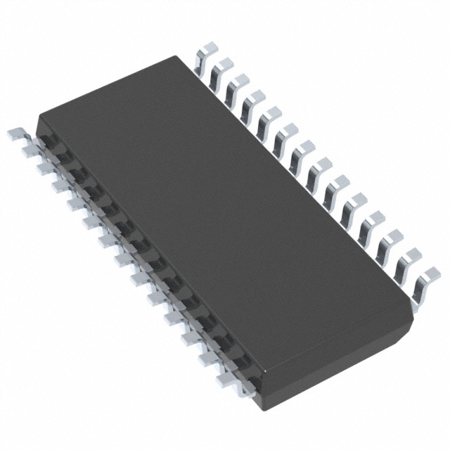
PACKAGE: SO-28
)
s
(
t
c
u
d
o
)
r
s
(
P
t
c
e
t
u
e
d
l
o
o
r
s
P
b
e
O
t
e
l
)
o
s
(
s
t
b
c
u
O
d
o
)
r
s
P
(
t
c
e
t
u
e
l
d
o
o
r
s
P
b
O
e
t
e
l
o
s
b
O
■
■
■
■
■
■
■
■
■
■
■
SO-28
ORDERING NUMBERS:L6917BD
L6917BDTR (Tape & Reel)
DESCRIPTION
The device is a power supply controller specifically
designed to provide a high performance DC/DC conversion for high current microprocessors.
The device implements a dual-phase step-down controller with a 180° phase-shift between each phase.
A precise 5-bit digital to analog converter (DAC) allows adjusting the output voltage from 1.100V to
1.850V with 25mV binary steps.
The high precision internal reference assures the selected output voltage to be within ±0.8%. The high
peak current gate drive affords to have fast switching
to the external power mos providing low switching
losses.
The device assures a fast protection against load
over current and load over/under voltage. An internal
crowbar is provided turning on the low side mosfet if
an over-voltage is detected. In case of over-current,
the system works in Constant Current mode.
APPLICATIONS
■ POWER SUPPLY FOR SERVERS AND
WORKSTATIONS
■ POWER SUPPLY FOR HIGH CURRENT
MICROPROCESSORS
■ DISTRIBUTED DC-DC CONVERTERS
BLOCK DIAGRAM
ROSC / INH
SGND
VCCDR
PGOOD
2 PHASE
OSCILLATOR
PWM1
+
DIGITAL
SOFT START
CURRENT
CORRECTION
-
CH 1 OVER
CURRENT
LOGIC PWM
ADAPTIVE ANTI
CROSS-CONDUCTION
BOOT1
UGATE1
HS
PHASE1
LGATE1
LS
ISEN1
VCC
VCCDR
LOGIC
AND
PROTECTIONS
TOTAL
CURRENT
CURRENT
READING
+
PGNDS1
PGND
VID4
VID3
AVG
CURRENT
CH2 OVER
CURRENT
VID0
ISEN2
FBR
+
10k
IFB
10k
10k
CH 2 OVER
CURRENT
PWM2
ERROR
AMPLIFIER
REMOTE
BUFFER
LOGIC PWM
ADAPTIVE ANTI
CROSS-CONDUCTION
CH1 OVER
CURRENT
10k
FBG
PGNDS2
CURRENT
READING
DAC
VID1
CURRENT
CORRECTION
VID2
LGATE2
LS
PHASE2
UGATE2
HS
Vcc
BOOT2
VSEN
September 2002
FB
COMP
Vcc
1/33
�L6917B
ABSOLUTE MAXIMUM RATINGS
Symbol
Vcc, VCCDR
VBOOT-VPHASE
Parameter
Value
Unit
to PGND
15
V
Boot Voltage
15
V
15
V
-0.3 to Vcc+0.3
V
-0.3 to 7
V
VUGATE1-VPHASE1
VUGATE2-VPHASE2
LGATE1, PHASE1, LGATE2, PHASE2 to PGND
All other pins to PGND
)
s
(
t
c
u
d
o
)
r
s
(
P
t
c
e
t
u
e
d
l
o
o
r
s
P
b
e
O
t
e
l
)
o
s
(
s
t
b
c
u
O
d
o
)
r
s
P
(
t
c
e
t
u
e
l
d
o
o
r
s
P
b
O
e
t
e
l
o
s
b
O
26
V
Value
Unit
Thermal Resistance Junction to Ambient
60
°C/W
Maximum junction temperature
150
°C
Storage temperature range
-40 to 150
°C
Junction Temperature Range
-25 to 125
°C
2
W
Vphase
Sustainable Peak Voltage t < 20ns @ 600kHz
THERMAL DATA
Symbol
Rth j-amb
Tmax
Tstorage
Tj
PMAX
Parameter
Max power dissipation at Tamb = 25°C
PIN CONNECTION
LGATE1
1
28
PGND
VCCDR
2
27
LGATE2
PHASE1
3
26
PHASE2
UGATE1
4
25
UGATE2
BOOT1
5
24
BOOT2
VCC
6
23
PGOOD
GND
7
22
VID4
COMP
8
21
VID3
FB
9
20
VID2
VSEN
10
19
VID1
FBR
11
18
VID0
FBG
12
17
OSC / INH / FAULT
ISEN1
13
16
ISEN2
PGNDS1
14
15
PGNDS2
SO28
2/33
�L6917B
ELECTRICAL CHARACTERISTICS
VCC = 12V ±10%, TJ = 0 to 70°C unless otherwise specified
Symbol
Parameter
Test Condition
Min
Typ
Max
Unit
Vcc SUPPLY CURRENT
Vcc supply current
HGATEx and LGATEx open
VCCDR=VBOOT=12V
7.5
10
12.5
mA
ICCDR
VCCDR supply current
LGATEx open; VCCDR=12V
2
3
4
mA
IBOOTx
Boot supply current
HGATEx open; PHASEx to PGND
VCC=VBOOT=12V
0.5
1
1.5
mA
ICC
)
s
(
t
c
u
d
o
)
r
s
(
P
t
c
e
t
u
e
d
l
o
o
r
s
P
b
e
O
t
e
l
)
o
s
(
s
t
b
c
u
O
d
o
)
r
s
P
(
t
c
e
t
u
e
l
d
o
o
r
s
P
b
O
e
t
e
l
o
s
b
O
POWER-ON
Turn-On VCC threshold
VCC Rising; VCCDR=5V
7.8
9
10.2
V
Turn-Off VCC threshold
VCC Falling; VCCDR=5V
6.5
7.5
8.5
V
Turn-On VCCDR
Threshold
VCCDR Rising
VCC=12V
4.2
4.4
4.6
V
Turn-Off VCCDR
Threshold
VCCDR Falling
VCC=12V
4.0
4.2
4.4
V
OSC = OPEN
OSC = OPEN; Tj=0°C to 125°C
278
270
300
322
330
kHz
kHz
RT to GND=74kΩ
450
500
550
kHz
0.9
V
OSCILLATOR/INHIBIT/FAULT
fOSC
Initial Accuracy
fOSC,Rosc Total Accuracy
INH
Inhibit threshold
ISINK=5mA
0.8
0.85
dMAX
Maximum duty cycle
OSC = OPEN
70
75
∆Vosc
Ramp Amplitude
1.8
2
2.2
V
FAULT
Voltage at pin OSC
OVP or UVP Active
4.75
5.0
5.25
V
Output Voltage
Accuracy
VID0, VID1, VID2, VID3, VID4
see Table1;
FBR = VOUT; FBG = GND
-0.8
-
0.8
%
VID pull-up Current
VIDx = GND
4
5
6
µA
VID pull-up Voltage
VIDx = OPEN
3.1
-
3.4
V
%
REFERENCE AND DAC
IDAC
ERROR AMPLIFIER
DC Gain
SR
80
dB
15
V/µs
DC Gain
1
V/V
Common Mode Rejection Ratio
40
dB
Slew-Rate
COMP=10pF
DIFFERENTIAL AMPLIFIER (REMOTE BUFFER)
CMRR
3/33
�L6917B
ELECTRICAL CHARACTERISTICS (continued)
VCC = 12V ±10%, TJ = 0 to 70°C unless otherwise specified
Symbol
SR
Parameter
Test Condition
Input Offset
FBR=1.100V to1.850V;
FBG=GND
Slew Rate
VSEN=10pF
Min
Typ
-12
Max
Unit
12
mV
15
V/µs
DIFFERENTIAL CURRENT SENSING
IISEN1,
IISEN2
Bias Current
IPGNDSx
IISEN1,
IISEN2
IFB
Iload=0
45
50
55
Bias Current
45
50
55
Bias Current at
Over Current Threshold
80
85
Active Droop Current
Iload35µA): the device enters in Quasi-Constant-Current operation. The low-side mosfets stays ON
until IINFO becomes lower than 35µA skipping clock cycles. The high side mosfets can be turned ON with a TON
imposed by the control loop at the next available clock cycle and the device works in the usual way until another
OCP event is detected.
The device limits the bottom of the inductor current triangular waveform. So the average current delivered can
slightly increase also in Over Current condition since the current ripple increases. In fact, the ON time increases
due to the OFF time rise because of the current has to reach the 140% bottom. The worst-case condition is
when the duty cycle reaches its maximum value (d=75% internally limited). When this happens, the device
works in Constant Current and the output voltage decrease as the load increase. Crossing the UVP threshold
causes the device to latch (FAULT pin is driven high).
Figure 5 shows this working condition
)
s
(
t
c
u
d
o
)
r
s
(
P
t
c
e
t
u
e
d
l
o
o
r
s
P
b
e
O
t
e
l
)
o
s
(
s
t
b
c
u
O
d
o
)
r
s
P
(
t
c
e
t
u
e
l
d
o
o
r
s
P
b
O
e
t
e
l
o
s
b
O
Figure 5. Constant Current operation
Ipeak
Vout
Droop
effect
IMAX
140%
TonMAX
UVP
TonMAX
Inom
IOCP
IMAX
Iout
It can be observed that the peak current (Ipeak) is greater than the 140% but it can be determined as follow:
V IN – Vout M IN
Ipea k = 1.4 ⋅ I NOM + --------------------------------------- ⋅ To n M AX
L
Where INOM is the nominal current and Vout MIN is the minimum output voltage (VID-40% as explained below).
The device works in Constant-Current, and the output voltage decreases as the load increase, until the output
voltage reaches the under-voltage threshold (VoutMIN). When this threshold is crossed, all mosfets are turned
off, the FAULT pin is driven high and the device stops working. Cycle the power supply to restart operation.
The maximum average current during the Constant-Current behavior results:
Ip eak – 1.4 ⋅ I NOM
I M AX = 1.4 ⋅ I NOM + 2 ⋅ ------------------------------------------------2
In this particular situation, the switching frequency results reduced. The ON time is the maximum allowed (TonMAX) while the OFF time depends on the application:
Ipe ak – 1.4 ⋅ INOM
1
f = ------------------------------------------T O FF = L ⋅ ------------------------------------------------Vout
To n M AX + T O FF
Over current is set anyway when IINFOx reaches 35µA. The full load value is only a convention to work with convenient values for IFB. Since the OCP intervention threshold is fixed, to modify the percentage with respect to
the load value, it can be simply considered that, for example, to have on OCP threshold of 170%, this will correspond to IINFOx = 35µA (IFB = 70µA). The full load current will then correspond to IINFOx = 20.5µA (IFB = 41µA).
12/33
�L6917B
Integrated Droop Function
The device uses a droop function to satisfy the requirements of high performance microprocessors, reducing
the size and the cost of the output capacitor.
This method "recovers" part of the drop due to the output capacitor ESR in the load transient, introducing a dependence of the output voltage on the load current
As shown in figure 6, the ESR drop is present in any case, but using the droop function the total deviation of the
output voltage is minimized. In practice the droop function introduces a static error (Vdroop in figure 6) proportional to the output current. Since the device has an average current mode regulation, the information about the
total current delivered is used to implement the Droop Function. This current (equal to the sum of both IINFOx)
is sourced from the FB pin. Connecting a resistor between this pin and Vout, the total current information flows
only in this resistor because the compensation network between FB and COMP has always a capacitor in series
(See fig. 7). The voltage regulated is then equal to:
)
s
(
t
c
u
d
o
)
r
s
(
P
t
c
e
t
u
e
d
l
o
o
r
s
P
b
e
O
t
e
l
)
o
s
(
s
t
b
c
u
O
d
o
)
r
s
P
(
t
c
e
t
u
e
l
d
o
o
r
s
P
b
O
e
t
e
l
o
s
b
O
VOUT = VID - RFB · IFB
Since IFB depends on the current information about the two phases, the output characteristic vs. load current is
given by:
R SENSE
V OUT = VID – R FB ⋅ ---------------------- ⋅ I OUT
Rg
Figure 6. Output transient response without (a) and with (b) the droop function
ESR DROP
ESR DROP
VMAX
VDROOP
VNOM
VMIN
(a)
(b)
Figure 7. Active Droop Function Circuit
RFB
COMP
To VOUT
FB
I FB
VPROG
The feedback current is equal to 50µA at nominal full load (IFB = IINFO1 + IINFO2) and 70µA at the OC threshold,
so the maximum output voltage deviation is equal to:
∆VFULL_POSITIVE_LOAD = +RFB · 50µA
∆VPOSITIVE_OC_THRESHOLD = +RFB · 70µA
Droop function is provided only for positive load; if negative load is applied, and then IINFOx < 0, no current is
sunk from the FB pin. The device regulates at the voltage programmed by the VID.
13/33
�L6917B
Output Voltage Protection and Power Good
The output voltage is monitored by pin VSEN. If it is not within +12/-10% (typ.) of the programmed value, the
powergood output is forced low. Power good is an open drain output and it is enabled only after the soft start is
finished (2048 clock cycles after start-up).
The device provides over voltage protection; when the voltage sensed by the V SEN pin reaches 2.1V (typ.), the
controller permanently switches on both the low-side mosfets and switches off both the high-side mosfets in order to protect the CPU. The OSC/INH/FAULT pin is driven high (5V) and power supply (Vcc) turn off and on is
required to restart operations. The over Voltage percentage is set by the ratio between the OVP threshold (set
at 2.1V) and the reference programmed by VID.
2.1V
O VP[%] = ----------------------------------------------------------------------------- ⋅ 100
Refer ence Voltage ( VID )
)
s
(
t
c
u
d
o
)
r
s
(
P
t
c
e
t
u
e
d
l
o
o
r
s
P
b
e
O
t
e
l
)
o
s
(
s
t
b
c
u
O
d
o
)
r
s
P
(
t
c
e
t
u
e
l
d
o
o
r
s
P
b
O
e
t
e
l
o
s
b
O
Under voltage protection is also provided. If the output voltage drops below the 60% of the reference voltage for
more than one clock period the device turns off and the FAULT pin is driven high.
Both Over Voltage and Under Voltage are active also during soft start (Under Voltage after than Vout reaches
0.8V). During soft-start the reference voltage used to determine the OV and UV thresholds is the increasing voltage driven by the 2048 soft start digital counter.
Remote Voltage Sense
A remote sense buffer is integrated into the device to allow output voltage remote sense implementation without
any additional external components. In this way, the output voltage programmed is regulated between the remote buffer inputs compensating motherboard trace losses or connector losses if the device is used for a VRM
module. The very low offset amplifier senses the output voltage remotely through the pins FBR and FBG (FBR
is for the regulated voltage sense while FBG is for the ground sense) and reports this voltage internally at VSEN
pin with unity gain eliminating the errors.
If remote sense is not required, the output voltage is sensed by the VSEN pin connecting it directly to the output
voltage. In this case the FBG and FBR pins must be connected anyway to the regulated voltage.
Input Capacitor
The input capacitor is designed considering mainly the input rms current that depends on the duty cycle as reported in figure 8. Considering the dual-phase topology, the input rms current is highly reduced comparing with
a single phase operation.
Rms Current Normalized (IRMS/IOUT)
Figure 8. Input rms Current vs. Duty Cycle (D) and Driving Relationships
0.50
Single Phase
Dual Phase
0.25
I rms =
I
OUT
⋅ 2D ⋅ (1 − 2D)
2
I
OUT
⋅ (2D - 1) ⋅ (2 − 2D)
2
if D < 0 .5
if D > 0.5
0.25
0.50
0.75
Duty Cycle (VOUT/VIN)
It can be observed that the input rms value is one half of the single-phase equivalent input current in the worst
case condition that happens for D = 0.25 and D = 0.75.
14/33
�L6917B
The power dissipated by the input capacitance is then equal to:
P RM S = ESR ⋅ ( I RM S )
2
Input capacitor is designed in order to sustain the ripple relative to the maximum load duty cycle. To reach the
high rms value needed by the CPU power supply application and also to minimize components cost, the input
capacitance is realized by more than one physical capacitor. The equivalent rms current is simply the sum of
the single capacitor's rms current.
Input bulk capacitor must be equally divided between high-side drain mosfets and placed as close as possible
to reduce switching noise above all during load transient. Ceramic capacitor can also introduce benefits in high
frequency noise decoupling, noise generated by parasitic components along power path.
)
s
(
t
c
u
d
o
)
r
s
(
P
t
c
e
t
u
e
d
l
o
o
r
s
P
b
e
O
t
e
l
)
o
s
(
s
t
b
c
u
O
d
o
)
r
s
P
(
t
c
e
t
u
e
l
d
o
o
r
s
P
b
O
e
t
e
l
o
s
b
O
Output Capacitor
Since the microprocessors require a current variation beyond 50A doing load transients, with a slope in the
range of tenth A/µs, the output capacitor is a basic component for the fast response of the power supply.
Dual phase topology reduces the amount of output capacitance needed because of faster load transient response (switching frequency is doubled at the load connections). Current ripple cancellation due to the 180°
phase shift between the two phases also reduces requirements on the output ESR to sustain a specified voltage
ripple.
When a load transient is applied to the converter's output, for first few microseconds the current to the load is
supplied by the output capacitors. The controller recognizes immediately the load transient and increases the
duty cycle, but the current slope is limited by the inductor value.
The output voltage has a first drop due to the current variation inside the capacitor (neglecting the effect of the
ESL):
∆VOUT = ∆IOUT · ESR
A minimum capacitor value is required to sustain the current during the load transient without discharge it. The
voltage drop due to the output capacitor discharge is given by the following equation:
2
∆I OUT ⋅ L
∆V OUT = --------------------------------------------------------------------------------------------2 ⋅ C OUT ⋅ ( V INM IN ⋅ D M AX – V OUT )
Where DMAX is the maximum duty cycle value. The lower is the ESR, the lower is the output drop during load
transient and the lower is the output voltage static ripple.
Inductor design
The inductance value is defined by a compromise between the transient response time, the efficiency, the cost
and the size. The inductor has to be calculated to sustain the output and the input voltage variation to maintain
the ripple current ∆IL between 20% and 30% of the maximum output current. The inductance value can be calculated with this relationship:
V IN – V OUT V OUT
L = ------------------------------ ⋅ --------------V IN
fs ⋅ ∆I L
Where fSW is the switching frequency, VIN is the input voltage and V OUT is the output voltage.
Increasing the value of the inductance reduces the ripple current but, at the same time, reduces the converter
response time to a load transient. The response time is the time required by the inductor to change its current
from initial to final value. Since the inductor has not finished its charging time, the output current is supplied by
the output capacitors. Minimizing the response time can minimize the output capacitance required.
The response time to a load transient is different for the application or the removal of the load: if during the application of the load the inductor is charged by a voltage equal to the difference between the input and the output
15/33
�L6917B
voltage, during the removal it is discharged only by the output voltage. The following expressions give approximate response time for ∆I load transient in case of enough fast compensation network response:
L ⋅ ∆I
t a pplic atio n = -----------------------------V IN – V OUT
L ⋅ ∆I
t rem ov al = --------------V OUT
The worst condition depends on the input voltage available and the output voltage selected. Anyway the worst
case is the response time after removal of the load with the minimum output voltage programmed and the maximum input voltage available.
Figure 9. Inductor ripple current vs Vout
9
L=1.5µH, Vin=12V
)
s
(
t
c
u
d
o
)
r
s
(
P
t
c
e
t
u
e
d
l
o
o
r
s
P
b
e
O
t
e
l
)
o
s
(
s
t
b
c
u
O
d
o
)
r
s
P
(
t
c
e
t
u
e
l
d
o
o
r
s
P
b
O
e
t
e
l
o
s
b
O
Inductor Ripple [A]
8
L=2µH,
Vin=12V
7
6
L=3µH,
Vin=12V
5
4
L=1.5µH,
Vin=5V
3
L=2µH,
Vin=5V
2
L=3µH, Vin=5V
1
0
0.5
1.5
2.5
3.5
Output Voltage [V]
MAIN CONTROL LOOP
The L6917B control loop is composed by the Current Sharing control loop and the Average Current Mode control loop. Each loop gives, with a proper gain, the correction to the PWM in order to minimize the error in its
regulation: the Current Sharing control loop equalize the currents in the inductors while the Average Current
Mode control loop fixes the output voltage equal to the reference programmed by VID. Figure 10 reports the
block diagram of the main control loop.
Figure 10. Main Control Loop Diagram
L1
+
PWM1
CURRENT
SHARING
DUTY CYCLE
CORRECTION
1/5
1/5
IINFO1
L2
+
PWM2
ERROR
AMPLIFIER
4/5
+
D02IN1392
REFERENCE
PROGRAMMED
BY VID
-
COMP
16/33
IINFO2
FB
ZF(S)
ZFB
CO
RO
�L6917B
■
Current Sharing (CS) Control Loop
Active current sharing is implemented using the information from Tran conductance differential amplifier in an
average current mode control scheme. A current reference equal to the average of the read current (IAVG) is
internally built; the error between the read current and this reference is converted to a voltage with a proper gain
and it is used to adjust the duty cycle whose dominant value is set by the error amplifier at COMP pin (See fig.
11).
The current sharing control is a high bandwidth control loop allowing current sharing even during load transients.
The current sharing error is affected by the choice of external components; choose precise Rg resistor (±1% is
necessary) to sense the current. The current sharing error is internally dominated by the voltage offset of Tran
conductance differential amplifier; considering a voltage offset equal to 2mV across the sense resistor, the current reading error is given by the following equation:
∆I RE AD
2mV
-------------------- = ---------------------------------------R SENSE ⋅ I M AX
I M AX
)
s
(
t
c
u
d
o
)
r
s
(
P
t
c
e
t
u
e
d
l
o
o
r
s
P
b
e
O
t
e
l
)
o
s
(
s
t
b
c
u
O
d
o
)
r
s
P
(
t
c
e
t
u
e
l
d
o
o
r
s
P
b
O
e
t
e
l
o
s
b
O
Where ∆IREAD is the difference between one phase current and the ideal current (IMAX/2).
For Rsense = 4mΩ and Imax = 40A the current sharing error is equal to 2.5%, neglecting errors due to Rg and
Rsense mismatches.
Figure 11. Current Sharing Control Loop
+
L1
PWM1
CURRENT
SHARING
DUTY CYCLE
CORRECTION
1/5
1/5
+
PWM2
IINFO2
IINFO1
L2
COMP
VOUT
D02IN1393
■
Average Current Mode (ACM) Control Loop
The average current mode control loop is reported in figure 12. The current information IFB sourced by the FB
pin flows into RFB implementing the dependence of the output voltage from the read current.
The ACM control loop gain results (obtained opening the loop after the COMP pin):
PWM ⋅ Z F ( s ) ⋅ ( R DROOP + Z P ( s ) )
G LO O P ( s ) = -------------------------------------------------------------------------------------------------------------------ZF (s )
1
( Z P ( s ) + Z L ( s ) ) ⋅ --------------- + 1 + ------------ ⋅ R FB
A(s)
A ( s )
Where:
R s en se
– R DROOP = ------------------- ⋅ R FB is the equivalent output resistance determined by the droop function;
Rg
– ZP(s) is the impedance resulting by the parallel of the output capacitor (and its ESR) and the applied
load Ro;
17/33
�L6917B
– ZF(s) is the compensation network impedance;
– ZL(s) is the parallel of the two inductor impedance;
– A(s) is the error amplifier gain;
4 ∆V IN
– PWM = --- ⋅ ------------------- · is the ACM PWM transfer function where DVosc is the oscillator ramp amplitude
5 ∆V O SC
and has a typical value of 2V
Removing the dependence from the Error Amplifier gain, so assuming this gain high enough, the control loop
gain results:
ZF ( s)
V IN
Rs Z P ( s )
4
G LO O P ( s ) = – --- ⋅ ------------------- ⋅ ------------------------------------ ⋅ -------- + ---------------
5 ∆V OS C Z P ( s ) + Z L ( s ) Rg R FB
)
s
(
t
c
u
d
o
)
r
s
(
P
t
c
e
t
u
e
d
l
o
o
r
s
P
b
e
O
t
e
l
)
o
s
(
s
t
b
c
u
O
d
o
)
r
s
P
(
t
c
e
t
u
e
l
d
o
o
r
s
P
b
O
e
t
e
l
o
s
b
O
With further simplifications, it results:
Z F ( s ) R o + R DROOP
V IN
1 + s ⋅ Co ⋅ ( R DROOP //Ro + ESR )
4
G L OO P ( s ) = – --- ⋅ ------------------- ⋅ --------------- ⋅ -------------------------------------- ⋅ ---------------------------------------------------------------------------------------------------------------------------------5 ∆V O SC R FB
RL
RL
2
L
L
R o + ------s ⋅ C o ⋅ --- + s ⋅ --------------- + Co ⋅ ESR + Co ⋅ ------- + 1
2
2
2
2 ⋅ Ro
Considering now that in the application of interest it can be assumed that Ro>>RL; ESR