®
L7800AB/AC SERIES
PRECISION 1A REGULATORS
s s
s s s s
OUTPUT CURRENT IN EXCESS OF 1 A OUTPUT VOLTAGES OF 5; 6; 8; 9; 12; 15; 18; 20; 24V THERMAL OVERLOAD PROTECTION OUTPUT TRANSITION SOA PROTECTION 2% OUTPUT VOLTAGE TOLERANCE GUARANTEED IN EXTENDED TEMPERATURE RANGE
DESCRIPTION The L7800A series of three-terminal positive regulators is available in TO-220 and D2PAK packages and several fixed output voltages, making it useful in a wide range of applications.These regulators can provide local on-card regulation, eliminating the distribution problems associated with single point regulation. Each type employs internal current limiting, thermal shut-down and safe area protection, making it essentially indestructible. If adequate heat sinking is provided, they can deliver over 1A output current. Although designed primarily as fixed voltage regulators, these devices can be used with external components to obtain adjustable voltages and currents. BLOCK DIAGRAM
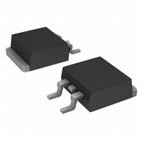
D2PAK
TO-220
November 1999
1/17
�L7800AB/AC
ABSOLUTE MAXIMUM RATINGS
Symbol Vi Io P tot T op T st g Parameter DC Input Voltage (for VO = 5 to 18V) (for V O = 20, 24V) Output Current Power Dissipation Operating Junction Temperature Range (for L7800AC) (for L7800AB ) Storage Temperature Range Value 35 40 Internally limited Internally limited 0 to 150 -40 to 125 - 65 to 150
o o o
Unit V V
C C C
THERMAL DATA
Symbol Parameter Max Max D PAK 3 62.5
2
TO-220 3 50
Unit
o o
R thj- ca se Thermal Resistance Junction-case R thj- amb Thermal Resistance Junction-ambient
C/W C/W
CONNECTION DIAGRAM AND ORDERING NUMBERS (top view)
TO-220 Type L7805AB L7805AC L7806AB L7806AC L7808AB L7808AC L7809AB L7809AC L7812AB L7812AC L7815AB L7815AC L7818AB L7818AC L7820AB L7820AC L7824AB L7824AC TO-220 L7805ABV L7805ACV L7806ABV L7806ACV L7808ABV L7808ACV L7809ABV L7809ACV L7812ABV L7812ACV L7815ABV L7815ACV L7818ABV L7818ACV L7820ABV L7820ACV L7824ABV L7824ACV D 2PAK (*) L7805ABD2T L7805ACD2T L7806ABD2T L7806ACD2T L7808ABD2T L7808ACD2T L7809ABD2T L7809ACD2T L7812ABD2T L7812ACD2T L7815ABD2T L7815ACD2T
D2PAK Output Voltage 5V 5V 6V 6V 8V 8V 9V 9V 12V 12V 15V 15V 18V 18V 24V 24V
(*) AVAILABLE IN TAPE AND REEL WITH ”-TR” SUFFIX
2/17
�L7800AB/AC
APPLICATION CIRCUIT
SCHEMATIC DIAGRAM
3/17
�L7800AB/AC
TEST CIRCUITS Figure 1 : DC Parameter Figure 2 : Load Regulation.
Figure 3 : Ripple Rejection.
4/17
�L7800AB/AC
ELECTRICAL CHARACTERISTICS FOR L7805A (Vi = 10V, Io = 1 A, Tj = 0 to 125 oC (L7805AC), Tj = -40 to 125 oC (L7805AB) unless otherwise specified)
Symbol Vo Vo ∆ Vo * Parameter Output Voltage Output Voltage Line Regulation Tj = 25 C Io = 5 mA to 1 A Vi = 7.5 to 20 V Vi = 7.5 to 25 V Vi = 8 to 12 V Vi = 8 to 12 V Vi = 7.3 to 20 V Po ≤ 15 W Io = 500 mA Tj = 25 oC Tj = 25 oC
o
Test Conditions
Min. 4.9 4.8
Typ. 5 5 7 10 2 7 25 30 8 4.3
Max. 5.1 5.2 50 5 25 50 100 100 50 6 6 0.8 0.8 0.5
Unit V V mV mV mV mV mV mV mV mA mA mA mA dB V µ V/V o mΩ A A mV/ oC
∆ Vo *
Load Regulation
Io = 5 mA to 1 A Io = 5 mA to 1.5 A Tj = 25 oC Io = 250 to 750 mA Tj = 25 C Vi = 8 to 25 V Io = 500 mA Tj = 25 oC Vi = 7.5 to 20 V Io = 5 mA to 1 A Vi = 8 to 18 V Io = 500 mA Io = 1 A f = 120 Hz
o
Id ∆Id
Quiescent Current Quiescent Current Change
SVR Vd eN Ro Is c I scp ∆ Vo
Supply Voltage Rejection Dropout Voltage Output Noise Voltage Output Resistance Short Circuit Current Short Circuit Peack Current Output Voltage Drift
68 2
Tj = 25 oC Tj = 25 C
o o
B = 10Hz to 100KHz f = 1KHz Vi = 35 V Tj = 25 C
o
10 17
Tamb = 25 C
0.2 2.2 -1.1
∆T
* Load and line regulation are specified at constant junction temperature. Changes in Vo due to heating effects must be taken into account separately. Pulse testing with low duty cycle is used.
5/17
�L7800AB/AC
ELECTRICAL CHARACTERISTICS FOR L7806A (Vi = 11V, Io = 1 A, Tj = 0 to 125 oC (L7806AC), Tj = -40 to 125 oC (L7806AB) unless otherwise specified)
Symbol Vo Vo ∆ Vo * Parameter Output Voltage Output Voltage Line Regulation Tj = 25 C Io = 5 mA to 1 A Vi = 8.6 to 21 V Vi = 8.6 to 25 V Vi = 9 to 13 V Vi = 9 to 13 V Vi = 8.3 to 21 V Po ≤ 15 W Io = 500 mA Tj = 25 oC Tj = 25 oC
o
Test Conditions
Min. 5.88 5.76
Typ. 6 6 9 11 3 9 25 30 10 4.3
Max. 6.12 6.24 60 60 30 60 100 100 50 6 6 0.8 0.8 0.5
Unit V V mV mV mV mV mV mV mV mA mA mA mA dB V µ V/V o mΩ A A mV/ oC
∆ Vo *
Load Regulation
Io = 5 mA to 1 A Io = 5 mA to 1.5 A Tj = 25 oC Io = 250 to 750 mA Tj = 25 oC Vi = 9 to 25 V Io = 500 mA Tj = 25 oC Vi = 8.6 to 21 V Io = 5 mA to 1 A Vi = 9 to 19 V Io = 500 mA Io = 1 A f = 120 Hz
Id ∆Id
Quiescent Current Quiescent Current Change
SVR Vd eN Ro Is c I scp ∆ Vo
Supply Voltage Rejection Dropout Voltage Output Noise Voltage Output Resistance Short Circuit Current Short Circuit Peack Current Output Voltage Drift
65 2
Tj = 25 oC Tj = 25 C
o o
B = 10Hz to 100KHz f = 1KHz Vi = 35 V Tj = 25 C
o
10 17
Tamb = 25 C
0.2 2.2 -0.8
∆T
* Load and line regulation are specified at constant junction temperature. Changes in Vo due to heating effects must be taken into account separately. Pulse testing with low duty cycle is used.
6/17
�L7800AB/AC
ELECTRICAL CHARACTERISTICS FOR L7808A (Vi = 14V, Io = 1 A, Tj = 0 to 125 oC (L7808AC), Tj = -40 to 125 oC (L7808AB) unless otherwise specified)
Symbol Vo Vo ∆ Vo * Parameter Output Voltage Output Voltage Line Regulation Tj = 25 C Io = 5 mA to 1 A Vi = 10.6 to 23 V Vi = 10.6 to 25 V Vi = 11 to 17 V Vi = 11 to 17 V Vi = 10.4 to 23 V Po ≤ 15 W Io = 500 mA Tj = 25 oC Tj = 25 oC
o
Test Conditions
Min. 7.84 7.7
Typ. 8 8 12 15 5 12 25 30 10 4.3
Max. 8.16 8.3 80 80 40 80 100 100 50 6 6 0.8 0.8 0.5
Unit V V mV mV mV mV mV mV mV mA mA mA mA dB V µ V/V o mΩ A A mV/ oC
∆Vo *
Load Regulation
Io = 5 mA to 1 A Io = 5 mA to 1.5 A Tj = 25 oC Io = 250 to 750 mA Tj = 25 oC Vi = 11 to 25 V Io = 500 mA Tj = 25 oC Vi = 10.6 to 23 V Io = 5 mA to 1 A Vi = 11.5 to 21.5 V Io = 500 mA Io = 1 A f = 120 Hz
Id ∆Id
Quiescent Current Quiescent Current Change
SVR Vd eN Ro Is c I scp ∆ Vo
Supply Voltage Rejection Dropout Voltage Output Noise Voltage Output Resistance Short Circuit Current Short Circuit Peack Current Output Voltage Drift
62 2
Tj = 25 oC Tj = 25 C
o o
B = 10Hz to 100KHz f = 1KHz Vi = 35 V Tj = 25 C
o
10 18
Tamb = 25 C
0.2 2.2 -0.8
∆T
* Load and line regulation are specified at constant junction temperature. Changes in Vo due to heating effects must be taken into account separately. Pulse testing with low duty cycle is used.
7/17
�L7800AB/AC
ELECTRICAL CHARACTERISTICS FOR L7809A (Vi = 15V, Io = 1 A, Tj = 0 to 125 oC (L7809AC), Tj = -40 to 125 oC (L7809AB) unless otherwise specified)
Symbol Vo Vo ∆ Vo * Parameter Output Voltage Output Voltage Line Regulation Tj = 25 C Io = 5 mA to 1 A Vi = 10.6 to 23 V Vi = 10.6 to 25 V Vi = 11 to 17 V Vi = 11 to 17 V Vi = 10.4 to 23 V Po ≤ 15 W Io = 500 mA Tj = 25 oC Tj = 25 oC
o
Test Conditions
Min. 8.82 8.65
Typ. 9 9 12 15 5 12 25 30 10 4.3
Max. 9.18 9.35 90 90 45 90 100 100 50 6 6 0.8 0.8 0.5
Unit V V mV mV mV mV mV mV mV mA mA mA mA dB V µ V/V o mΩ A A mV/ oC
∆Vo *
Load Regulation
Io = 5 mA to 1 A Io = 5 mA to 1.5 A Tj = 25 oC Io = 250 to 750 mA Tj = 25 oC Vi = 11 to 25 V Io = 500 mA Tj = 25 oC Vi = 10.6 to 23 V Io = 5 mA to 1 A Vi = 11.5 to 21.5 V Io = 500 mA Io = 1 A f = 120 Hz
Id ∆Id
Quiescent Current Quiescent Current Change
SVR Vd eN Ro Is c I scp ∆ Vo
Supply Voltage Rejection Dropout Voltage Output Noise Voltage Output Resistance Short Circuit Current Short Circuit Peack Current Output Voltage Drift
61 2
Tj = 25 oC Tj = 25 C
o o
B = 10Hz to 100KHz f = 1KHz Vi = 35 V Tj = 25 C
o
10 18
Tamb = 25 C
0.2 2.2 -0.8
∆T
* Load and line regulation are specified at constant junction temperature. Changes in Vo due to heating effects must be taken into account separately. Pulse testing with low duty cycle is used.
8/17
�L7800AB/AC
ELECTRICAL CHARACTERISTICS FOR L7812A (Vi = 19V, Io = 1 A, Tj = 0 to 125 oC (L7812AC), Tj = -40 to 125 oC (L7812AB) unless otherwise specified)
Symbol Vo Vo ∆ Vo * Parameter Output Voltage Output Voltage Line Regulation Tj = 25 C Io = 5 mA to 1 A Vi = 14.8 to 27 V Vi = 14.8 to 30 V Vi = 16 to 22 V Vi = 16 to 22 V Vi = 14.5 to 27 V Po ≤ 15 W Io = 500 mA Tj = 25 oC Tj = 25 oC
o
Test Conditions
Min. 11.75 11.5
Typ. 12 12 13 16 6 13 25 30 10 4.4
Max. 12.25 12.5 120 120 60 120 100 100 50 6 6 0.8 0.8 0.5
Unit V V mV mV mV mV mV mV mV mA mA mA mA dB V µ V/V o mΩ A A mV/ oC
∆Vo *
Load Regulation
Io = 5 mA to 1 A Io = 5 mA to 1.5 A Tj = 25 oC Io = 250 to 750 mA Tj = 25 oC Vi = 15 to 30 V Io = 500 mA Tj = 25 oC Vi = 14.8 to 27 V Io = 5 mA to 1 A Vi = 15 to 25 V Io = 500 mA Io = 1 A f = 120 Hz
Id ∆Id
Quiescent Current Quiescent Current Change
SVR Vd eN Ro Is c I scp ∆ Vo
Supply Voltage Rejection Dropout Voltage Output Noise Voltage Output Resistance Short Circuit Current Short Circuit Peack Current Output Voltage Drift
60 2
Tj = 25 oC Tj = 25 C
o o
B = 10Hz to 100KHz f = 1KHz Vi = 35 V Tj = 25 C
o
10 18
Tamb = 25 C
0.2 2.2 -1
∆T
* Load and line regulation are specified at constant junction temperature. Changes in Vo due to heating effects must be taken into account separately. Pulse testing with low duty cycle is used.
9/17
�L7800AB/AC
ELECTRICAL CHARACTERISTICS FOR L7815A (Vi = 23V, Io = 1 A, Tj = 0 to 125 oC (L7815AC), Tj = -40 to 125 oC (L7815AB) unless otherwise specified)
Symbol Vo Vo ∆ Vo * Parameter Output Voltage Output Voltage Line Regulation Tj = 25 C Io = 5 mA to 1 A Vi = 17.9 to 30 V Vi = 17.9 to 30 V Vi = 20 to 26 V Vi = 20 to 26 V Vi = 17.5 to 30 V Po ≤ 15 W Io = 500 mA Tj = 25 oC Tj = 25 oC
o
Test Conditions
Min. 14.7 14.4
Typ. 15 15 13 16 6 13 25 30 10 4.4
Max. 15.3 15.6 150 150 75 150 100 100 50 6 6 0.8 0.8 0.5
Unit V V mV mV mV mV mV mV mV mA mA mA mA dB V µ V/V o mΩ A A mV/ oC
∆Vo *
Load Regulation
Io = 5 mA to 1 A Io = 5 mA to 1.5 A Tj = 25 oC Io = 250 to 750 mA Tj = 25 oC Vi = 17.5 to 30 V Vi = 17.5 to 30 V Io = 5 mA to 1 A Vi = 18.5 to 28.5 V Io = 500 mA Io = 1 A Io = 500 mA Tj = 25 oC f = 120 Hz
Id ∆Id
Quiescent Current Quiescent Current Change
SVR Vd eN Ro Is c I scp ∆ Vo
Supply Voltage Rejection Dropout Voltage Output Noise Voltage Output Resistance Short Circuit Current Short Circuit Peack Current Output Voltage Drift
58 2
Tj = 25 oC Tj = 25 C
o o
B = 10Hz to 100KHz f = 1KHz Vi = 35 V Tj = 25 C
o
10 19
Tamb = 25 C
0.2 2.2 -1
∆T
* Load and line regulation are specified at constant junction temperature. Changes in Vo due to heating effects must be taken into account separately. Pulse testing with low duty cycle is used.
10/17
�L7800AB/AC
ELECTRICAL CHARACTERISTICS FOR L7818A (Vi = 27V, Io = 1 A, Tj = 0 to 125 oC (L7818AC), Tj = -40 to 125 oC (L7818AB) unless otherwise specified)
Symbol Vo Vo ∆ Vo * Parameter Output Voltage Output Voltage Line Regulation Tj = 25 C Io = 5 mA to 1 A Vi = 21 to 33 V Po ≤ 15 W
o
Test Conditions
Min. 17.64 17.3
Typ. 18 18 25 28 10 5 25 30 10 4.5
Max. 18.36 18.7 180 180 90 180 100 100 50 6 6 0.8 0.8 0.5
Unit V V mV mV mV mV mV mV mV mA mA mA mA dB V µ V/V o mΩ A A mV/ oC
Vi = 21 to 33 V Io = 500 mA Vi = 24 to 30 V Vi = 24 to 30 V Tj = 25 oC Vi = 20.6 to 33 V Tj = 25 oC Io = 5 mA to 1 A Io = 5 mA to 1.5 A Tj = 25 oC Io = 250 to 750 mA Tj = 25 oC Vi = 21 to 33 V Vi = 21 to 33 V Io = 5 mA to 1 A Vi = 22 to 32 V Io = 500 mA Io = 1 A Io = 500 mA Tj = 25 oC f = 120 Hz
∆Vo *
Load Regulation
Id ∆Id
Quiescent Current Quiescent Current Change
SVR Vd eN Ro Is c I scp ∆ Vo
Supply Voltage Rejection Dropout Voltage Output Noise Voltage Output Resistance Short Circuit Current Short Circuit Peack Current Output Voltage Drift
57 2
Tj = 25 oC Tj = 25 C
o o
B = 10Hz to 100KHz f = 1KHz Vi = 35 V Tj = 25 C
o
10 19
Tamb = 25 C
0.2 2.2 -1
∆T
* Load and line regulation are specified at constant junction temperature. Changes in Vo due to heating effects must be taken into account separately. Pulse testing with low duty cycle is used.
11/17
�L7800AB/AC
ELECTRICAL CHARACTERISTICS FOR L7820A (Vi = 28V, Io = 1 A, Tj = 0 to 125 oC (L7820AC), Tj = -40 to 125 oC (L7820AB) unless otherwise specified)
Symbol Vo Vo ∆ Vo * Parameter Output Voltage Output Voltage Line Regulation Tj = 25 C Io = 5 mA to 1 A Vi = 23 to 35 V Vi = 23 to 35 V Vi = 26 to 32 V Vi = 26 to 32 V Vi = 23 to 32 V Po ≤ 15 W Io = 500 mA Tj = 25 oC Tj = 25 oC 25 30 10 4.5 Io = 500 mA Tj = 25 oC f = 120 Hz 56 2 Tj = 25 C
o o o
Test Conditions
Min. 19.6 19.2
Typ. 20 20
Max. 20.4 20.8 200 200 100 200 100 100 50 6 6 0.8 0.8 0.5
Unit V V mV mV mV mV mV mV mV mA mA mA mA dB V µ V/V o mΩ A A mV/ oC
∆Vo *
Load Regulation
Io = 5 mA to 1 A Io = 5 mA to 1.5 A Tj = 25 oC Io = 250 to 750 mA Tj = 25 oC Vi = 23 to 35 V Vi = 23 to 35 V Io = 5 mA to 1 A Vi = 24 to 35 V Io = 500 mA Io = 1 A
Id ∆Id
Quiescent Current Quiescent Current Change
SVR Vd eN Ro Is c I scp ∆ Vo
Supply Voltage Rejection Dropout Voltage Output Noise Voltage Output Resistance Short Circuit Current Short Circuit Peack Current Output Voltage Drift
Tj = 25 oC
B = 10Hz to 100KHz f = 1KHz Vi = 35 V Tj = 25 C
o
10 20
Tamb = 25 C
0.2 2.2 -1
∆T
* Load and line regulation are specified at constant junction temperature. Changes in Vo due to heating effects must be taken into account separately. Pulse testing with low duty cycle is used.
12/17
�L7800AB/AC
ELECTRICAL CHARACTERISTICS FOR L7824A (Vi = 33V, Io = 1 A, Tj = 0 to 125 oC (L7824AC), Tj = -40 to 125 oC (L7824AB) unless otherwise specified)
Symbol Vo Vo ∆ Vo * Parameter Output Voltage Output Voltage Line Regulation Tj = 25 C Io = 5 mA to 1 A Vi = 27.3 to 38 V Po ≤ 15 W
o
Test Conditions
Min. 23.5 23
Typ. 24 24 31 35 14 31 25 30 10 4.6
Max. 24.5 25 240 240 120 240 100 100 50 6 6 0.8 0.8 0.5
Unit V V mV mV mV mV mV mV mV mA mA mA mA dB V µ V/V o mΩ A A mV/ oC
Vi = 27 to 38 V Io = 500 mA Vi = 30 to 36 V Vi = 30 to 36 V Tj = 25 oC Vi = 26.7 to 38 V Tj = 25 oC Io = 5 mA to 1 A Io = 5 mA to 1.5 A Tj = 25 oC Io = 250 to 750 mA Tj = 25 oC Vi = 27.3 to 38 V Vi = 27.3 to 38 V Io = 5 mA to 1 A Vi = 28 to 38 V Io = 500 mA Io = 1 A Io = 500 mA Tj = 25 oC f = 120 Hz
∆Vo *
Load Regulation
Id ∆Id
Quiescent Current Quiescent Current Change
SVR Vd eN Ro Is c I scp ∆ Vo
Supply Voltage Rejection Dropout Voltage Output Noise Voltage Output Resistance Short Circuit Current Short Circuit Peack Current Output Voltage Drift
54 2
Tj = 25 oC Tj = 25 C
o o
B = 10Hz to 100KHz f = 1KHz Vi = 35 V Tj = 25 C
o
10 20
Tamb = 25 C
0.2 2.2 -1.5
∆T
* Load and line regulation are specified at constant junction temperature. Changes in Vo due to heating effects must be taken into account separately. Pulse testing with low duty cycle is used.
13/17
�L7800AB/AC
APPLICATIONS INFORMATION DESIGN CONSIDERATIONS The L7800A Series of fixed voltage regulators are designed with Thermal Overload Protection that shuts down the circuit when subjected to an excessive power overload condition, Internal Short-circuit Protection that limits the maximum current the circuit will pass, and Output Transistor Safe-Area Compensation that reduces the output short-circuit current as the voltage across the pass transistor is increased. In many low current applications, compensation capacitors are not required. However, it is recommended that the regulator input be bypassed with a capacitor if the regulator is Figure 4 : Current Regulator. connected to the power supply filter with long wire lengths, or if the output load capacitance is large. An input bypass capacitor should be selected to provide good high-frequency characteristics to insure stable operation under all load conditions. A 0.33µF or larger tantalum, mylar, or other capacitor having low internal impedance at high frequencies should be chosen. The bypass capacitor should be mounted with the shortest possible leads directly across the regulators input terminals. Normally good construction techniques should be used to minimize ground loops and lead resistance drops since the regulator has no external sense lead. Figure 5 : Adjustable Output Regulator.
VO, 7.0V to 20V Vi – VO ≥ 2.0V
IO =
V XX +Id R1
The addition of an operational amplifier allows adjustment to higher or intermediate values while retaining regulation characteristics. The minimum voltage obtainable with this arrangement is 2.0V greater than the regulator voltage. Figure 7 : Short-circuit Protection.
Figure 6 : Current Boost Regulator.
R1 =
V BEQ1 I REQ −
I Q1 β Q1 V BEQ1
R1
)
IO = I
REG
+ Q 1 ( I REG −
The circuit of figure 6 can be modified to provide supply protection against short circuit by adding a short-circuit sense resistor, Rsc, and an additional PNP transistor. The current sensing PNP must be able to handle the short-circuit current of the three-terminal regulator. Therefore, a four-ampere plastic power transistor is specified.
14/17
�L7800AB/AC
TO-220 MECHANICAL DATA
DIM. MIN. A C D D1 E F F1 F2 G G1 H2 L2 L4 L5 L6 L7 L9 DIA. 13.0 2.65 15.25 6.2 3.5 3.75 0.49 0.61 1.14 1.14 4.95 2.4 10.0 16.4 14.0 2.95 15.75 6.6 3.93 3.85 0.511 0.104 0.600 0.244 0.137 0.147
E
mm TYP. MAX. 4.60 1.32 2.72 1.27 0.70 0.88 1.70 1.70 5.15 2.7 10.40 0.019 0.024 0.044 0.044 0.194 0.094 0.393 MIN. 0.173 0.048 0.094 4.40 1.23 2.40
inch TYP. MAX. 0.181 0.051 0.107 0.050 0.027 0.034 0.067 0.067 0.203 0.106 0.409 0.645 0.551 0.116 0.620 0.260 0.154 0.151
A
C
D1
L2 F1
D
G1
Dia. F2 F
L5 L7 L6
L9
L4
G
H2
P011C
15/17
�L7800AB/AC
TO-263 (D2PAK) MECHANICAL DATA
mm MIN. A A1 B B2 C C2 D E G L L2 L3 4.4 2.49 0.7 1.14 0.45 1.23 8.95 10 4.88 15 1.27 1.4 TYP. MAX. 4.6 2.69 0.93 1.7 0.6 1.36 9.35 10.4 5.28 15.85 1.4 1.75 MIN. 0.173 0.098 0.027 0.044 0.017 0.048 0.352 0.393 0.192 0.590 0.050 0.055 inch TYP. MAX. 0.181 0.106 0.036 0.067 0.023 0.053 0.368 0.409 0.208 0.624 0.055 0.068
DIM.
D A C A2 DETAIL”A” A1 B2 B G
C2
DETAIL”A”
E
L2
L
L3
P011P6/F
16/17
�L7800AB/AC
Information furnished is believed to be accurate and reliable. However, STMicroelectronic s assumes no responsibility for the consequences of use of such information nor for any infringement of patents or other rights of third parties which may result from its use. No license is granted by implication or otherwise under any patent or patent rights of STMicroelectronics. Specification mentioned in this publication are subject to change without notice. This publication supersedes and replaces all information previously supplied. STMicroelectronics products are not authorized for use as critical components in life support devices or systems withoutexpress written approval of STMicroelectronics. The ST logo is a registered trademark of STMicroelectronics © 1999 STMicroelectronics – Printed in Italy – All Rights Reserved STMicroelectronics GROUP OF COMPANIES Australia - Brazil - China - Finland - France - Germany - Hong Kong - India - Italy - Japan - Malaysia - Malta - Morocco Singapore - Spain - Sweden - Switzerland - United Kingdom - U.S.A. http://www.st.com .
17/17
�


 工商网监
湘ICP备2023018690号
工商网监
湘ICP备2023018690号
