L7980
2 A step-down switching regulator
Datasheet - production data
Industrial:
– PLD, PLA, FPGA, chargers
Networking: XDSL, modems, DC-DC modules
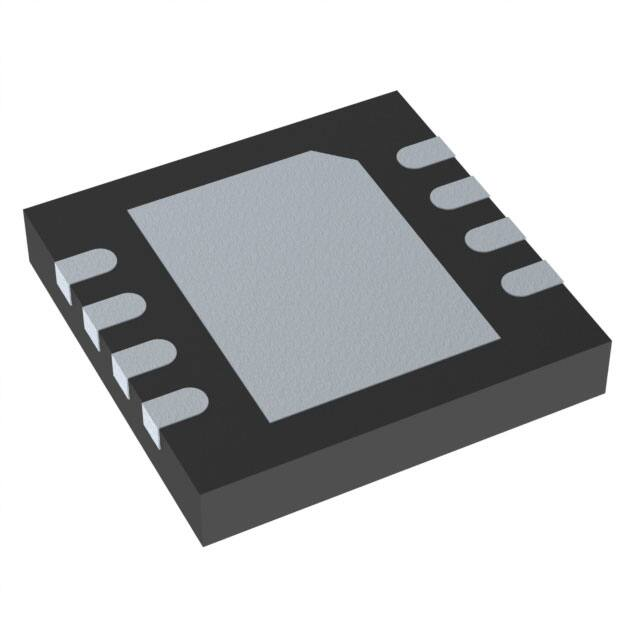
VFQFPN8 3 x 3
HSOP8 exposed pad
Computer:
– Optical storage, hard disk drive, printers,
audio/graphic cards
LED driving
Features
2 A DC output current
Description
4.5 V to 28 V input voltage
The L7980 device is a step-down switching
regulator with a 2.5 A (minimum) current limited
embedded Power MOSFET, so it is able to deliver
up to 2 A current to the load depending on the
application conditions.
Output voltage adjustable from 0.6 V
250 kHz switching frequency, programmable
up to 1 MHz
Internal soft-start and enable
The input voltage can range from 4.5 V to 28 V,
while the output voltage can be set starting from
0.6 V to VIN.
Low dropout operation: 100% duty cycle
Voltage feed-forward
Zero load current operation
Overcurrent and thermal protection
VFQFPN 3 x 3 - 8L and HSOP8 package
Applications
Consumer:
– STB, DVD, DVD recorder, car audio, LCD
TV and monitors
Requiring a minimum set of external components,
the device includes an internal 250 kHz switching
frequency oscillator that can be externally
adjusted up to 1 MHz.
The QFN and the HSOP packages with exposed
pad allow reducing the RthJA down to 60 °C/W
and 40 °C/W respectively.
Figure 1. Application circuit
May 2014
This is information on a product in full production.
DocID15181 Rev 6
1/42
www.st.com
�Contents
L7980
Contents
1
Pin settings . . . . . . . . . . . . . . . . . . . . . . . . . . . . . . . . . . . . . . . . . . . . . . . . 4
1.1
Pin connection . . . . . . . . . . . . . . . . . . . . . . . . . . . . . . . . . . . . . . . . . . . . . . 4
1.2
Pin description . . . . . . . . . . . . . . . . . . . . . . . . . . . . . . . . . . . . . . . . . . . . . . 4
2
Maximum ratings . . . . . . . . . . . . . . . . . . . . . . . . . . . . . . . . . . . . . . . . . . . . 5
3
Thermal data . . . . . . . . . . . . . . . . . . . . . . . . . . . . . . . . . . . . . . . . . . . . . . . 5
4
Electrical characteristics . . . . . . . . . . . . . . . . . . . . . . . . . . . . . . . . . . . . . 6
5
Functional description . . . . . . . . . . . . . . . . . . . . . . . . . . . . . . . . . . . . . . . 8
6
7
2/42
5.1
Oscillator and synchronization . . . . . . . . . . . . . . . . . . . . . . . . . . . . . . . . . . 9
5.2
Soft-start . . . . . . . . . . . . . . . . . . . . . . . . . . . . . . . . . . . . . . . . . . . . . . . . . . .11
5.3
Error amplifier and compensation . . . . . . . . . . . . . . . . . . . . . . . . . . . . . . 12
5.4
Overcurrent protection . . . . . . . . . . . . . . . . . . . . . . . . . . . . . . . . . . . . . . . 12
5.5
Enable function . . . . . . . . . . . . . . . . . . . . . . . . . . . . . . . . . . . . . . . . . . . . 14
5.6
Hysteretic thermal shutdown . . . . . . . . . . . . . . . . . . . . . . . . . . . . . . . . . . 14
Application informations . . . . . . . . . . . . . . . . . . . . . . . . . . . . . . . . . . . . 15
6.1
Input capacitor selection . . . . . . . . . . . . . . . . . . . . . . . . . . . . . . . . . . . . . . 15
6.2
Inductor selection . . . . . . . . . . . . . . . . . . . . . . . . . . . . . . . . . . . . . . . . . . . 16
6.3
Output capacitor selection . . . . . . . . . . . . . . . . . . . . . . . . . . . . . . . . . . . . 17
6.4
Compensation network . . . . . . . . . . . . . . . . . . . . . . . . . . . . . . . . . . . . . . . 19
6.4.1
Type III compensation network . . . . . . . . . . . . . . . . . . . . . . . . . . . . . . . 20
6.4.2
Type II compensation network . . . . . . . . . . . . . . . . . . . . . . . . . . . . . . . . 23
6.5
Thermal considerations . . . . . . . . . . . . . . . . . . . . . . . . . . . . . . . . . . . . . . 27
6.6
Layout considerations . . . . . . . . . . . . . . . . . . . . . . . . . . . . . . . . . . . . . . . 28
6.7
Application circuit . . . . . . . . . . . . . . . . . . . . . . . . . . . . . . . . . . . . . . . . . . . 30
Application ideas . . . . . . . . . . . . . . . . . . . . . . . . . . . . . . . . . . . . . . . . . . . 34
7.1
Positive buck-boost . . . . . . . . . . . . . . . . . . . . . . . . . . . . . . . . . . . . . . . . . 34
7.2
Inverting buck-boost . . . . . . . . . . . . . . . . . . . . . . . . . . . . . . . . . . . . . . . . . 36
DocID15181 Rev 6
�L7980
Contents
8
Package information . . . . . . . . . . . . . . . . . . . . . . . . . . . . . . . . . . . . . . . . 38
9
Order codes . . . . . . . . . . . . . . . . . . . . . . . . . . . . . . . . . . . . . . . . . . . . . . . 41
10
Revision history . . . . . . . . . . . . . . . . . . . . . . . . . . . . . . . . . . . . . . . . . . . 41
DocID15181 Rev 6
3/42
42
�Pin settings
L7980
1
Pin settings
1.1
Pin connection
Figure 2. Pin connection (top view)
OUT
VCC
SYNCH
GND
EN
FSW
COMP
1.2
FB
Pin description
Table 1. Pin description
4/42
No.
Type
1
OUT
Description
Regulator output
2
SYNCH
Master/slave synchronization. When it is left floating, a signal with
a phase shift of half a period respect to the power turn on is present at
the pin. When connected to an external signal at a frequency higher than
the internal one, then the device is synchronized by the external signal,
with zero phase shift.
Connecting together the SYNCH pin of two devices, the one with higher
frequency works as master and the other one as slave; so the two
powers turn on have a phase shift of half a period.
3
EN
A logical signal (active high) enable the device. With EN higher than
1.2 V the device is ON and with EN is lower than 0.3 V the device is OFF.
4
COMP
5
FB
Feedback input. Connecting the output voltage directly to this pin the
output voltage is regulated at 0.6 V. To have higher regulated voltages an
external resistor divider is required from Vout to the FB pin.
6
FSW
The switching frequency can be increased connecting an external
resistor from the FSW pin and ground. If this pin is left floating the device
works at its free-running frequency of 250 kHz.
7
GND
Ground
8
VCC
Unregulated DC input voltage
Error amplifier output to be used for loop frequency compensation
DocID15181 Rev 6
�L7980
2
Maximum ratings
Maximum ratings
Table 2. Absolute maximum ratings
Symbol
3
Parameter
Vcc
Input voltage
OUT
Output DC voltage
Value
Unit
30
-0.3 to VCC
FSW, COMP, SYNCH
Analog pin
-0.3 to 4
EN
Enable pin
-0.3 to VCC
FB
Feedback voltage
-0.3 to 1.5
PTOT
Power dissipation
at TA < 60 °C
VFQFPN
1.5.
HSOP
2
V
W
TJ
Junction temperature range
-40 to 150
°C
Tstg
Storage temperature range
-55 to 150
°C
Thermal data
Table 3. Thermal data
Symbol
RthJA
Parameter
Maximum thermal resistance
junction ambient(1)
Value
VFQFPN
60
HSOP
40
Unit
°C/W
1. Package mounted on demonstration board.
DocID15181 Rev 6
5/42
42
�Electrical characteristics
4
L7980
Electrical characteristics
TJ = 25 °C, VCC = 12 V, unless otherwise specified.
Table 4. Electrical characteristics
Values
Symbol
Parameter
Test condition
Unit
Min.
Operating input voltage range
(1)
Turn on VCC threshold
(1)
VCCHYS
VCC UVLO hysteresis
(1)
RDSON
MOSFET on resistance
VCC
VCCON
ILIM
4.5
Max.
28
4.4
0.12
V
0.35
160
180
160
250
2.5
3.0
3.5
225
250
275
(1)
Maximum limiting current
Typ.
m
A
Oscillator
FSW
Switching frequency
VFSW
FSW pin voltage
D
FADJ
(1)
275
1.254
Duty cycle
Adjustable switching frequency
220
0
RFSW = 33 k
KHz
V
100
1000
%
KHz
Dynamic characteristics
VFB
Feedback voltage
4.5 V < VCC < 28 V(1)
0.593
0.6
0.607
V
2.4
mA
30
A
DC characteristics
IQ
IQST-BY
Quiescent current
Duty cycle = 0, VFB = 0.8 V
Total standby quiescent current
20
Enable
EN threshold voltage
EN current
Device OFF level
Device ON level
0.3
1.2
EN = VCC
7.5
10
8.2
9.1
V
A
Soft-start
TSS
Soft-start duration
FSW pin floating
7.4
FSW = 1 MHz, RFSW = 33 k
2
ms
Error amplifier
VCH
High level output voltage
VFB < 0.6 V
VCL
Low level output voltage
VFB > 0.6 V
IO SOURCE Source COMP pin
6/42
VFB = 0.5 V, VCOMP = 1 V
DocID15181 Rev 6
3
0.1
17
V
mA
�L7980
Electrical characteristics
Table 4. Electrical characteristics (continued)
Values
Symbol
Parameter
Test condition
Unit
Min.
IO SINK
GV
Sink COMP pin
VFB = 0.7 V, VCOMP = 1 V
Open loop voltage gain
(2)
Typ.
Max.
25
mA
100
dB
Synchronization function
High input voltage
2
3.3
Low input voltage
1
Slave sink current
VSYNCH = 2.9 V
Master output amplitude
ISOURCE = 4.5 mA
Output pulse width
SYNCH floating
Input pulse width
0.7
0.9
2.0
V
mA
V
110
70
ns
Protection
TSHDN
Thermal shutdown
150
Hysteresis
30
°C
1. Specification referred to TJ from -40 to +125 °C. Specification in the -40 to +125 °C temperature range are assured by
design, characterization and statistical correlation.
2. Guaranteed by design.
DocID15181 Rev 6
7/42
42
�Functional description
5
L7980
Functional description
The L7980 device is based on a “voltage mode”, constant frequency control. The output
voltage VOUT is sensed by the feedback pin (FB) compared to an internal reference (0.6 V)
providing an error signal that, compared to a fixed frequency sawtooth, controls the on and
off time of the power switch.
The main internal blocks are shown in the block diagram in Figure 3. They are:
A fully integrated oscillator that provides sawtooth to modulate the duty cycle and the
synchronization signal. Its switching frequency can be adjusted by an external resistor.
The voltage and frequency feed forward are implemented.
The soft-start circuitry to limit inrush current during the start-up phase.
The voltage mode error amplifier
The pulse width modulator and the relative logic circuitry necessary to drive the internal
power switch.
The high-side driver for embedded P-channel Power MOSFET switch.
The peak current limit sensing block, to handle overload and short-circuit conditions.
A voltage regulator and internal reference. It supplies internal circuitry and provides
a fixed internal reference.
A voltage monitor circuitry (UVLO) that checks the input and internal voltages.
A thermal shutdown block, to prevent thermal runaway.
Figure 3. Block diagram
VCC
REGULATOR
TRIMMING
EN
&
BANDGAP
EN
1.254V
3.3V
0.6V
COMP
UVLO
PEAK
CURRENT
LIMIT
THERMAL
SOFTSTART
SHUTDOWN
E/A
PWM
DRIVER
S
Q
R
OUT
OSCILLATOR
FB
8/42
FSW
GND
DocID15181 Rev 6
SYNCH
&
PHASE SHIFT
SYNCH
�L7980
5.1
Functional description
Oscillator and synchronization
Figure 4 shows the block diagram of the oscillator circuit. The internal oscillator provides
a constant frequency clock. Its frequency depends on the resistor externally connect to the
FSW pin. In case the FSW pin is left floating the frequency is 250 kHz; it can be increased
as shown in Figure 6 by external resistor connected to ground.
To improve the line transient performance, keeping the PWM gain constant versus the input
voltage, the voltage feed forward is implemented by changing the slope of the sawtooth
according to the input voltage change (see Figure 5.a).
The slope of the sawtooth also changes if the oscillator frequency is increased by the
external resistor. In this way a frequency feed forward is implemented (Figure 5.b) in order
to keep the PWM gain constant versus the switching frequency (see Section 6.4 on page 19
for PWM gain expression).
On the SYNCH pin the synchronization signal is generated. This signal has a phase shift of
180° with respect to the clock. This delay is useful when two devices are synchronized
connecting the SYNCH pin together. When SYNCH pins are connected, the device with
higher oscillator frequency works as the master, so the slave device switches at the
frequency of the master but with a delay of half a period. This minimizes the RMS current
flowing through the input capacitor (see the L5988D datasheet).
Figure 4. Oscillator circuit block diagram
Clock
FSW
Clock
Generator
Synchronization
SYNCH
Ramp
Generator
Sawtooth
The device can be synchronized to work at higher frequency feeding an external clock
signal. The synchronization changes the sawtooth amplitude, changing the PWM gain
(Figure 5.c). This changing has to be taken into account when the loop stability is studied.
To minimize the change of the PWM gain, the free running frequency should be set (with
a resistor on the FSW pin) only slightly lower than the external clock frequency. This preadjusting of the frequency will change the sawtooth slope in order to get negligible the
truncation of sawtooth, due to the external synchronization.
DocID15181 Rev 6
9/42
42
�Functional description
L7980
Figure 5. Sawtooth: voltage and frequency feed forward; external synchronization
Figure 6. Oscillator frequency versus FSW pin resistor
10/42
DocID15181 Rev 6
�L7980
5.2
Functional description
Soft-start
The soft-start is essential to assure a correct and safe startup of the step-down converter. It
avoids inrush current surge and makes the output voltage increases monothonically.
The soft-start is performed by a staircase ramp on the non inverting input (VREF) of the error
amplifier. So the output voltage slew rate is:
Equation 1
R1
SR OUT = SR VREF 1 + --------
R2
where SRVREF is the slew rate of the non inverting input, while R1and R2 is the resistor
divider to regulate the output voltage (see Figure 7). The soft-start stair case consists of
64 steps of 9.5 mV each one, from 0 V to 0.6 V. The time base of one step is of 32 clock
cycles. So the soft-start time and then the output voltage slew rate depend on the switching
frequency.
Figure 7. Soft-start scheme
Soft-start time results:
Equation 2
32 64
SS TIME = ----------------Fsw
For example with a switching frequency of 250 kHz the SSTIME is 8 ms.
DocID15181 Rev 6
11/42
42
�Functional description
5.3
L7980
Error amplifier and compensation
The error amplifier (E/A) provides the error signal to be compared with the sawtooth to
perform the pulse width modulation. Its non inverting input is internally connected to a 0.6 V
voltage reference, while its inverting input (FB) and output (COMP) are externally available
for feedback and frequency compensation. In this device the error amplifier is a voltage
mode operational amplifier so with high DC gain and low output impedance.
The uncompensated error amplifier characteristics are the following:
Table 5. Uncompensated error amplifier characteristics
Parameter
Value
Low frequency gain
100 dB
GBWP
4.5 MHz
Slew rate
7 V/s
Output voltage swing
0 to 3.3 V
Maximum source/sink current
17 mA/25 mA
In continuous conduction mode (CCM), the transfer function of the power section has two
poles due to the LC filter and one zero due to the ESR of the output capacitor. Different
kinds of compensation networks can be used depending on the ESR value of the output
capacitor. In case the zero introduced by the output capacitor helps to compensate the
double pole of the LC filter a type II compensation network can be used. Otherwise, a type
III compensation network has to be used (see Section 6.4 on page 19 for details about the
compensation network selection).
Anyway the methodology to compensate the loop is to introduce zeros to obtain a safe
phase margin.
5.4
Overcurrent protection
The L7980 device implements the overcurrent protection sensing current flowing through
the Power MOSFET. Due to the noise created by the switching activity of the Power
MOSFET, the current sensing is disabled during the initial phase of the conduction time.
This avoids an erroneous detection of a fault condition. This interval is generally known as
“masking time” or “blanking time”. The masking time is about 200 ns.
When the overcurrent is detected, two different behaviors are possible depending on the
operating condition.
12/42
1.
Output voltage in regulation. When the overcurrent is sensed, the Power MOSFET is
switched off and the internal reference (VREF), that biases the non inverting input of the
error amplifier, is set to zero and kept in this condition for a soft-start time (TSS, 2048
clock cycles). After this time, a new soft-start phase takes place and the internal
reference begins ramping (see Figure 8.a).
2.
Soft-start phase. If the overcurrent limit is reached the Power MOSFET is turned off
implementing the pulse by pulse overcurrent protection. During the soft-start phase,
under overcurrent condition, the device can skip pulses in order to keep the output
current constant and equal to the current limit. If at the end of the “masking time” the
current is higher than the overcurrent threshold, the Power MOSFET is turned off and it
will skip one pulse. If, at the next switching on at the end of the “masking time” the
DocID15181 Rev 6
�L7980
Functional description
current is still higher than the threshold, the device will skip two pulses. This
mechanism is repeated and the device can skip up to seven pulses. While, if at the end
of the “masking time” the current is lower than the overcurrent threshold, the number of
skipped cycles is decreased of one unit. At the end of soft-start phase the output
voltage is in regulation and if the overcurrent persists the behavior explained above
takes place (see Figure 8.b).
So the overcurrent protection can be summarized as an “hiccup” intervention when the
output is in regulation and a constant current during the soft-start phase. If the output is
shorted to ground when the output voltage is on regulation, the overcurrent is triggered and
the device starts cycling with a period of 2048 clock cycles between “hiccup” (Power
MOSFET off and no current to the load) and “constant current” with very short on-time and
with reduced switching frequency (up to one eighth of normal switching frequency). See
Figure 32 on page 33 for short-circuit behavior.
Figure 8. Overcurrent protection strategy
DocID15181 Rev 6
13/42
42
�Functional description
5.5
L7980
Enable function
The enable feature allows to put in standby mode the device. With the EN pin lower than
0.3 V the device is disabled and the power consumption is reduced to less than 30 µA. With
the EN pin lower than 1.2 V, the device is enabled. If the EN pin is left floating, an internal
pull down ensures that the voltage at the pin reaches the inhibit threshold and the device is
disabled. The pin is also VCC compatible.
5.6
Hysteretic thermal shutdown
The thermal shutdown block generates a signal that turns off the power stage if the junction
temperature goes above 150 °C. Once the junction temperature goes back to about 130 °C,
the device restarts in normal operation. The sensing element is very close to the PDMOS
area, so ensuring an accurate and fast temperature detection.
14/42
DocID15181 Rev 6
�L7980
Application informations
6
Application informations
6.1
Input capacitor selection
The capacitor connected to the input has to be capable to support the maximum input
operating voltage and the maximum RMS input current required by the device. The input
capacitor is subject to a pulsed current, the RMS value of which is dissipated over its ESR,
affecting the overall system efficiency.
So the input capacitor must have an RMS current rating higher than the maximum RMS
input current and an ESR value compliant with the expected efficiency.
The maximum RMS input current flowing through the capacitor can be calculated as:
Equation 3
2
2
2D
D
I RMS = I O D – --------------- + ------2
Where IO is the maximum DC output current, D is the duty cycle, is the efficiency.
Considering , this function has a maximum at D = 0.5 and it is equal to IO/2.
In a specific application the range of possible duty cycles has to be considered in order to
find out the maximum RMS input current. The maximum and minimum duty cycles can be
calculated as:
Equation 4
V OUT + V F
D MAX = ------------------------------------V INMIN – V SW
and
Equation 5
V OUT + V F
D MIN = -------------------------------------V INMAX – V SW
Where VF is the forward voltage on the freewheeling diode and VSW is voltage drop across
the internal PDMOS.
The peak to peak voltage across the input capacitor can be calculated as:
Equation 6
IO
D
D
V PP = ------------------------- 1 – ---- D + ---- 1 – D + ESR I O
C IN F SW
where ESR is the equivalent series resistance of the capacitor.
DocID15181 Rev 6
15/42
42
�Application informations
L7980
Given the physical dimension, ceramic capacitors can meet well the requirements of the
input filter sustaining a higher input RMS current than electrolytic / tantalum types. In this
case the equation of CIN as a function of the target VPP can be written as follows:
Equation 7
IO
D
D
C IN = --------------------------- 1 – ---- D + ---- 1 – D
V PP F SW
neglecting the small ESR of ceramic capacitors.
Considering = 1, this function has its maximum in D = 0.5, thus, given the maximum peak
to peak input voltage (VPP_MAX), the minimum input capacitor (CIN_MIN) value is:
Equation 8
IO
C IN_MIN = -----------------------------------------------2 V PP_MAX F SW
Typically CIN is dimensioned to keep the maximum peak-peak voltage in the order of 1% of
VINMAX
In Table 6 some multi layer ceramic capacitors suitable for this device are reported:
Table 6. Input MLCC capacitors
Manufacture
Taiyo Yuden
Murata
Series
Cap value (F)
Rated voltage (V)
UMK325BJ106MM-T
10
50
GMK325BJ106MN-T
10
35
GRM32ER71H475K
4.7
50
A ceramic bypass capacitor, as close to the VCC and GND pins as possible, so that
additional parasitic ESR and ESL are minimized, is suggested in order to prevent instability
on the output voltage due to noise. The value of the bypass capacitor can go from 100 nF to
1 µF.
6.2
Inductor selection
The inductance value fixes the current ripple flowing through the output capacitor. So the
minimum inductance value in order to have the expected current ripple has to be selected.
The rule to fix the current ripple value is to have a ripple at 20% - 40% of the output current.
In the continuous current mode (CCM), the inductance value can be calculated by Equation
9:
Equation 9
V IN – V OUT
V OUT + V F
I L = ------------------------------ T ON = ---------------------------- T OFF
L
L
Where TON is the conduction time of the internal high-side switch and TOFF is the
conduction time of the external diode [in CCM, FSW = 1 / (TON + TOFF)]. The maximum
current ripple, at fixed Vout, is obtained at maximum TOFF that is at minimum duty cycle
(see Section 6.1 to calculate minimum duty).
16/42
DocID15181 Rev 6
�L7980
Application informations
So fixing IL = 20% to 30% of the maximum output current, the minimum inductance value
can be calculated:
Equation 10
V OUT + V F 1 – D MIN
L MIN = ---------------------------- ----------------------I MAX
F SW
where FSW is the switching frequency, 1 / (TON + TOFF).
For example for VOUT = 5 V, VIN = 24 V, IO = 2 A and FSW = 250 kHz the minimum
inductance value to have IL = 30% of IO is about 28 H.
The peak current through the inductor is given by:
Equation 11
I L
I L PK = I O + -------2
So if the inductor value decreases, the peak current (that has to be lower than the current
limit of the device) increases. The higher is the inductor value, the higher is the average
output current that can be delivered, without reaching the current limit.
In Table 7 some inductor part numbers are listed.
Table 7. Inductors
Manufacturer
Coilcraft
Wurth
SUMIDA
6.3
Series
Inductor value (H)
Saturation current (A)
MSS1038
3.8 to 10
3.9 to 6.5
MSS1048
12 to 22
3.84 to 5.34
MSS1060
22 to 47
5 to 6.8
PD Type L
8.2 to 15
3.75 to 6.25
PD Type M
2.2 to 4.7
4 to 6
PD4 Type X
22 to 47
2.6 to 3.5
CDRH6D226/HP
1.5 to 3.3
3.6 to 5.2
CDR10D48MN
6.6 to 12
4.1 to 5.7
Output capacitor selection
The current in the capacitor has a triangular waveform which generates a voltage ripple
across it. This ripple is due to the capacitive component (charge or discharge of the output
capacitor) and the resistive component (due to the voltage drop across its ESR). So the
output capacitor has to be selected in order to have a voltage ripple compliant with the
application requirements.
The amount of the voltage ripple can be calculated starting from the current ripple obtained
by the inductor selection.
DocID15181 Rev 6
17/42
42
�Application informations
L7980
Equation 12
I MAX
V OUT = ESR I MAX + ------------------------------------8 C OUT f SW
Usually the resistive component of the ripple is much higher than the capacitive one, if the
output capacitor adopted is not a multi layer ceramic capacitor (MLCC) with very low ESR
value.
The output capacitor is important also for loop stability: it fixes the double LC filter pole and
the zero due to its ESR. In Section 6.4, it will be illustrated how to consider its effect in the
system stability.
For example with VOUT = 5 V, VIN = 24 V, IL = 0.6 A (resulting by the inductor value), in
order to have a VOUT = 0.01 · VOUT, if the multi layer ceramic capacitor are adopted, 10 µF
are needed and the ESR effect on the output voltage ripple can be neglected. In case of not
negligible ESR (electrolytic or tantalum capacitors), the capacitor is chosen taking into
account its ESR value. So in case of 220 with ESR = 50 m, the resistive component of the
drop dominates and the voltage ripple is 33 mV
The output capacitor is also important to sustain the output voltage when a load transient
with high slew rate is required by the load. When the load transient slew rate exceeds the
system bandwidth the output capacitor provides the current to the load. So if the high slew
rate load transient is required by the application the output capacitor and system bandwidth
have to be chosen in order to sustain the load transient.
In Table 8 some capacitor series are listed.
Table 8. Output capacitors
Manufacturer
Series
Cap value (F)
Rated voltage (V)
ESR (m)
GRM32
22 to 100
6.3 to 25