L9348
QUAD LOW SIDE DRIVER
s s s s s
s s s s s
SUPPLY VOLTAGE RANGE: 4.8 TO 18V OUTPUT VOLTAGE UP TO 40V OUTPUT VOLTAGE CLAMP DURING RECIRCULATION OF INDUCTIVE LOADS OUTPUT CURRENT CAPABILITY 2 X 5A AND 2 X 3A LOW POWER DISSIPATION DURING RECIRCULATION OF INDUCTIVE LOADS BY INTEGRATED FREE WHEELING DIODES (3A-DRIVERS ONLY) LOW ON-RESISTANCE 2 X 0.2Ω , 2 X 0.35Ω (TYP.) OUTPUT SHORT CIRCUIT CURRENT PROTECTION REAL TIME DIAGNOSTIC FUNCTIONS OVERTEMPERATURE SHUTDOWN SIGNAL- AND POWER-GROUND-LOSS SHUTDOWN
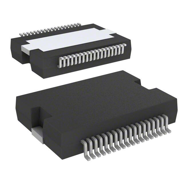
PowerSO-36 BARE DIE ORDERING NUMBERS: L9348 L9348-DIE1
s
3.3V CMOS COMPATIBLE INPUTS AND STATUS
DESCRIPTION The L9348 is a monolithic integrated quad low side driver realized in advanced Multipower-BCD technology. It is intended to drive inductive loads (relays, electromagnetic valves) in automotive and industrial applications.
Figure 1. Block Diagram
VS
VS Voltage Regulator + – VDD VCC VREG
=
C 166kHz
VDD
EN VS
EN FAIL ≥1
Q1
IN1
Diagnostic
OL SCP TSD GL
VREG
PGND1 5A - DRIVER CHANNEL1
ST1
PWRES
IN2 ST2 ENA
C 166kHz PWRES
EN
CHANNEL2
VDD VS
Q2 PGND2
EN
PWRES
PWRES
C 166kHz
C 166kHz
VDD
EN VS
EN FAIL ≥1
D3 Q3
IN3
Diagnostic
OL SCP TSD GL FB
VREG
PGND3 3A - DRIVER CHANNEL3
ST3
PWRES
IN4 ST4
99AT0073
C 166kHz PWRES
EN
D4 CHANNEL4 Q4 PGND4
GND
March 2002
1/13
�L9348
Figure 2. Pin Connection
N.C. PGND3 Q3 D3 Q1 Q2 D4 Q4 PGND4 N.C.
99AT0074
1 2 3 4 5 6 7 8 9 10 11 12 13 14 15 16 17 18
36 35 34 33 32 31 30 29 28 27 26 25 24 23 22 21 20 19
N.C. ST3 IN1 IN3 ST1 PGND1 N.C. VS GND PGND2 ENA ST2 IN4 IN2 ST4 N.C.
Table 1. Pin Description
N° 1, 18, 19, 36 2, 3 4, 5 6, 7 8, 9 10, 11 12, 13 14, 15 16, 17 20 21 22 23 24 25, 26 27 28 29 30, 31 32 33 34 Pin N.C. PGND3 Q3 D3 Q1 Q2 D4 Q4 PGND4 ST4 IN2 IN4 ST2 ENA PGND2 GND VS N.C. PGND1 ST1 IN3 IN1 (GND) Power Ground Channel 3 Power Output Channel 3 (3A switch) Recirculation Diode Channel 3 Power Output Channel 1 (5A switch) Power Output Channel 2 (5A switch) Recirculation Diode Channel 4 Power Output Channel 4 (3A switch) Power Ground Channel 4 Status Output Channel 4 Control Input Channel 2 Control Input Channel 4 Status Output Channel 2 Enable Power Ground Channel 2 Signal Ground Supply Voltage Not Connected Power Output Channel 3 Status Output Channel 1 Control Input Channel 3 Control Input Channel 1 Function
2/13
�L9348
Table 2. Thermal Data
Values Symbol Tj Tjc Tstg Parameter Junction temperature Junction temperature during clamping (life time) Storage temperature Test Conditions Min. -40 Typ. Max. 150 175 190 -55 150 2 °C °C °C °C °C/W Unit
Σt = 30min Σt = 15min
Rth j-case Thermal resistance junction to case
Table 3. Absolute Maximum Ratings The absolute maximum ratings are the limiting values for this device. Damage may occur if this device is subjected to conditions which are beyond these values.
Symbol Voltages VS VQ, VD VIN, VEN VST VDRmax Supply voltage range max. static Output voltage Input voltage range (IN1 to IN4, EN) Status output voltage range max. Reverse breakdown voltage free wheeling diodes D3, D4 Output current at reversal supply for Q1, Q2 Output current at reversal supply for Q3, Q4 Status output current range max. Discharging energy for inductive loads per channel Q1, Q2 max. load current free wheeling diodes Tj = 25°C Tj = 150°C t < 5ms |II | < 10mA |II | < 1mA IR = 100 µA -0.3 to 40 40 -1.5 to 6 -0.3 to 6 55 V V V V V Parameter Test Conditions Value Unit
Currents IQ 1/2 IQ 3/4 IST EQ1/2 -4 -2 -1 to 1 50 30 3 A A mA mJ mJ A
IFDmax ESD Protection
Supply and Signal pins Output pins (QX, DX)
versus GND versus common ground (=short of SGND with all PGND)
±2 ±4
kV kV
Note: Human Body Model according to MIL883C. The device withstands ST1 class level.
Table 4. Operating Range.
Symbol VS Tj Parameter Supply voltage Junction temperature Test Conditions Values Min. 4.8 -40 Typ. Max. 18 150 Unit V °C
3/13
�L9348
Table 5. Electrical Characteristcs The electrical characteristics are valid within the operating range (Table 4), unless otherwise specified
Symbol Power Supply IS IQ ID3/4 Supply current Quiescent current (outputs OFF) Quiescent current at pins D3/4 V IN1...IN4, ENA = H VENA = L VD3/4 ≤ 18V; VIN3/4 = L 10 8 6 400 mA mA Parameter Test Condition Min. Typ. Max. Unit
µA
Diagnostic Functions VQU1 to 4 Output open load voltage threshold IQU1 to 4 IQO1/2 IQO3/4 Tth Thy VthPGL VthSGL Output open load current threshold Overload current threshold Q 1, 2 Overload current threshold Q 3, 4 Overtemperature shutdown threshold Overtemperature hysteresis Power-GND-loss threshold Signal-GND-loss threshold 1.5 150 VS ≥ 6.5V VEN = X; VIN = L VS ≥ 6.5V VEN = H; VIN = H VS ≥ 6.5V VS ≥ 6.5V
2)
0.3
0.33
0.36
x VS mA
50
140
5 3 175
7.5 5
9 8 210
A A °C °C
10 2.5 330 3.5 510
V mV
Power Outputs (Q1 to Q4) RDSON1/2 Static drain-source ON-resistance Q1, Q2 IQ = 1A; VS ≥ 9.5V Tj = 25°C Tj = 125°C 3) Tj = 150°C 4) RDSON3,4 Static drain-source ON-resistance Q3, Q4 IQ = 1A; VS ≥ 9.5V Tj = 25°C Tj = 125°C 3) Tj = 150°C 4) VZ Z-diode clamping voltage = threshold of flyback detection Q3/4 Clamping voltage IQ ≥ 100mA, pos. supply VD3/4 IQ ≥ 100mA, neg. supply VD3/4 VENA = H, VIN = L 45 0.35 0.2
Ω
0.5 0.5
Ω Ω
Ω
0.75 0.75 60
Ω Ω V
VC IPD
4
10
V
Output pull down current
10
20
50
µA
4/13
�L9348
Table 5. Electrical Characteristcs The electrical characteristics are valid within the operating range (Table 4), unless otherwise specified
Symbol IQlk Parameter Output leakage current Test Condition V ENA = L,Tj = 25°C Tj = 125°C VFD3/4 RPD0 Forward voltage of free wheeling diodes D3, D4 Gate pull down resistor for nonsupplied VS ID3/4 = -1.5A VS = 0V, VD3/4 ≥ 6.5V 0.5 0.3 Min. Typ. Max. 1 5 1.75 3 Unit
µA µA
V kΩ
Timings tON tf tOFF tr tDSO tD tfilter tOLOFF Output ON delay time Output ON fall time Output OFF delay time Output OFF rise time Overload switch-OFF delay time Output OFF status delay time error detection filter time OLOFF error detection filter time
2)
IQ = 1A 1) IQ = 1A 1) IQ = 1A 1) IQ = 1A 1)
0 0.5 0 0.5 6 0.75 5.8 20
5 1.5 10 1.5 30 1.5
20 8 30 5 65 2.25 35 70
µs µs µs µs µs
ms
µs µs
Digital Inputs (IN1 to IN4, ENA) VIL VIH VIHy IIN Input low voltage Input high voltage Input voltage hysteresis Input pull down current
2)
-1.5 2 50 8 100 20
1 6
V V mV
VIN = 5V, VS ≥ 6.5V
40
µA
Digital Outputs (ST1 to ST4) VSTL VSTH Status output voltage in low state
5)
IST ≤ 40µA IST ≥ -40µA IST ≥ -120µA
0 2.5 2 0.3 1.5 0.64 3.2
0.4 3.45 3.45 1.5 7
V V V kΩ kΩ
Status output voltage in high state
5)
RDIAGL RDIAGH
ROUT + RDSON in low state ROUT + RDSON in high state
(1).See chapter 2.0 Timing Diagrams; resistive load condition; V S ≥ 9V (2).This parameter will not be tested but assured by design (3).Wafer-measurement (4).Measured on P-SO36 devices (5).Short circuit between two digital outputs (one in high the other in low state) will lead to the defined result "LOW"
5/13
�L9348
1.0 FUNCTIONAL DESCRIPTION 1.1 Overview
The four low-side switches are designed to drive inductive loads (relays, electromagnetic valves). For the 3A switches (Q3/4) integrated free-wheeling diodes (D3/4) are available and can be used as recirculation path for inductive loads. If either integrated nor external free-wheeling diodes are used the output voltage is clamped internally during discharge of inductive loads. The switches are controlled by CMOS compatible inputs (IN1-4) if the enable input is set to “high”. The status of each switch is monitored by the related status output (ST1-4). 1.2 Input Circuits
The control and enable inputs are active high, featuring switching thresholds with hysteresis and pull-down current sources. Not connected inputs are interpreted as “LOW”. If the enable input is set to “LOW” the outputs are switched off independent of the control input state (IN1-4). 1.3 Switching Stages
The four power outputs consist of DMOS-power transistors. The output stages are protected against short circuit to supply. Integrated output voltage clamp limits the output voltage in case of inductive load current flyback. Internal pull down current sources are provided at the outputs to assure a defined conditon in OFF mode. They will be disconnected in the disable mode (ENA=L). If the supply of the device gets lost but the loads and D3/4 are still supplied, an internal pull down resistor discharges the gate of the DMOS-power transistor to avoid switch on due to capacitive coupling. 1.4 Status Outputs
The CMOS compatible status outputs indicate the state of the drivers (LOW-level indicates driver in OFF state, HIGH-level indicates driver in ON state). If an error occurs the status output voltage changes like described in chapter 1.6 Error Detection. 1.5 Protective Circuits
The outputs are protected against current overload, overtemperature, and Power-GND-loss. 1.6 Error Detection
Two main error types are distinguished in the diagnostic logic. If current overload, overtemperature, signalGND-loss or a power-GND-loss occurs, the status output signal is inverted, an internal register is set and the driver is shutdown. The reset is done by switching off the corresponding control input or the enable input for at least the time tD (defined to 1.5ms typ.). See also Figure 6 in chapter 2.0 Timing Diagrams. All other errors (openload, active output voltage clamp) only cause an inverted status output signal but no shutdown of the driver. An internal register is set too, but the reset is triggered automatically after the time t D, if the error condition is no longer valid (see Figure 7 and Figure 8). Excepting the detection of the active output voltage clamp all errors are digitally filtered before they are interpreted by the diagnostic logic. The table 6 below shows the different failure conditions monitored in ON and OFF state: Table 6.
ON State ENA = HIGH, IN = HIGH Overloading of output (also shorted load to supply) Open load (under voltage detection) X X OFF State ENA = HIGH, IN = LOW typ. Filter time 18µs 44µs Reset done by
ENA or INx = “LOW” for t ≥ 1.5ms (typ.) internal timer (1.5ms typ.)
6/13
�L9348
Table 6.
ON State ENA = HIGH, IN = HIGH Open load (under current detection) Overtemperature Power-GND-loss Signal-GND-loss Output voltage clamp active (Q3/4 only) X X X X X X X OFF State ENA = HIGH, IN = LOW typ. Filter time 18µs 18µs 18µs 18µs Reset done by
internal timer (1.5ms typ.) ENA or INx = “LOW” for t ≥ 1.5ms (typ.) ENA or INx = “LOW” for t ≥ 1.5ms (typ.) ENA or INx = “LOW” for t ≥ 1.5ms (typ.) internal timer (1.5ms typ.)
1.7
Diagnostic Output at Pulse Width Operation (PWM)
If an input is operated with a pulsed signal (f ≥ 1/tD = 667 Hz typ.), the status does not follow each single pulse. An internal delay tD of typ. 1.5ms leads to a continuous status output signal (see Figure 4 in chapter 2.0 Timing Diagrams). 1.8 Diagnostic Table
In general the diagnostic follows the input signal in normal operating conditions. If any error is detected the diagnostic is inverted. Table 7.
Operating Condition Enable Input ENA L L H H L L H H H H H –> L H H H H –> L H Control Input IN L H/PWM L H/PWM L H/PWM L H/PWM H/PWM H/PWM X H/PWM –> L H/PWM H/PWM X H/PWM –> L Power Output Q OFF OFF OFF ON OFF OFF OFF ON OFF OFF OFF OFF OFF OFF OFF OFF Status Output ST L L L H X X H L L L L L L L L L
Normal function
Open load or short to ground
Overload or short to supply Latched overload Reset latch Overtemperature Latched overtemperature Reset latch
7/13
�L9348
2.0 TIMING DIAGRAMS Figure 3. Output slope with Resistive Load
VIN
t tON VQ
100% V Q 85% V Q 15% V Q
99AT0061
tf
tOFF
tr
note: parameters are not shown proportionally
t
Figure 4. Diagnostic Output at PWM operation
VIN
t IQ
IQU
t
VST
tD
tD
t
delayed status signal
99AT0063
note: parameters are not shown proportionally
8/13
�L9348
Figure 5. Overload Detection
VIN
overload detected
t IQ
IQO driver shut down IQU
t tDSO tfilter VST
error condition signalized
t
99AT0062
note: parameters are not shown proportionally
Figure 6. Driver Shut Down in Case of Overload
VIN
driver is shuted down and locked
tD IQ
IQO
t
driver is now free again
t
VST
error is signalized
99AT0064
tD
note: parameters are not shown proportionally
t
9/13
�L9348
Figure 7. Under Current Condition
VIN
t IQ
IQU
tfilter
under current condition detected
t
VST
under current condition signalized
tD
t
status signal is changed by internal reset
99AT0065
note: parameters are not shown proportionally
Figure 8. Open Load Condition in Off State
VIN
t VQ
VQU
tdetection
openload condition detected but not signalized due to: tdetection < t OLOFF
tOLOFF
tdetection
t tOLOFF
openload condition detected and signalized due to: tdetection > t OLOFF
VST
tD
99AT0066
t
note: parameters are not shown proportionally
10/13
�L9348
Figure 9. Output Voltage Clamp Detection
VIN3/4
t VQ3/4
VZ
t
VST3/4
tclamp
tclamp tD
t
time between two clamping periods is shorter than internal delay time -> status signal remains low
99AT0067
note: parameters are not shown proportionally
3.0 PAD POSITIONS Chip Size: 5.17 x 2.76 mm2 Figure 10.
PGND4 Q4 D4 Q2 Q1 D3 Q3 PGND3
ST4
IN2
IN4
ST2
ENA
PGND2
GND
VS
PGND1
ST1
IN3
IN1
ST3
11/13
�L9348
mm TYP. inch TYP.
DIM. A a1 a2 a3 b c D (1) D1 E e e3 E1 (1) E2 E3 E4 G H h L N S
MIN. 0.10 0 0.22 0.23 15.80 9.40 13.90
MAX. 3.60 0.30 3.30 0.10 0.38 0.32 16.00 9.80 14.50
MIN. 0.004 0 0.008 0.009 0.622 0.370 0.547
MAX. 0.141 0.012 0.130 0.004 0.015 0.012 0.630 0.385 0.570
OUTLINE AND MECHANICAL DATA
0.65 11.05 10.90 5.80 2.90 0 15.50 0.80 11.10 0.429 2.90 6.20 0.228 3.20 0.114 0.10 0 15.90 0.610 1.10 1.10 0.031 10°(max.) 8 °(max.)
0.0256 0.435 0.437 0.114 0.244 0.126 0.004 0.626 0.043 0.043
PowerSO36
(1): "D" and "E1" do not include mold flash or protrusions - Mold flash or protrusions shall not exceed 0.15mm (0.006 inch) - Critical dimensions are "a3", "E" and "G".
N
N a2 A DETAIL A e3 H lead e A a1 E DETAIL A
c DETAIL B
D a3
36 19
slug BOTTOM VIEW E3
B E2 E1 DETAIL B
0.35 Gage Plane
D1
1
1
8
-C-
S h x 45˚ b
⊕ 0.12
M
L
SEATING PLANE G C
AB
PSO36MEC
(COPLANARITY)
12/13
�L9348
Information furnished is believed to be accurate and reliable. However, STMicroelectronics assumes no responsibility for the consequences of use of such information nor for any infringement of patents or other rights of third parties which may result from its use. No license is granted by implication or otherwise under any patent or patent rights of STMicroelectronics. Specifications mentioned in this publication are subject to change without notice. This publication supersedes and replaces all information previously supplied. STMicroelectronics products are not authorized for use as critical components in life support devices or systems without express written approval of STMicroelectronics. The ST logo is a registered trademark of STMicroelectronics ® 2002 STMicroelectronics - All Rights Reserved STMicroelectronics GROUP OF COMPANIES Australia - Brazil - Canada - China - Finland - France - Germany - Hong Kong - India - Israel - Italy - Japan -Malaysia - Malta - Morocco Singapore - Spain - Sweden - Switzerland - United Kingdom - United States. http://www.st.com
13/13
�


 工商网监
湘ICP备2023018690号
工商网监
湘ICP备2023018690号
