L9362
QUAD LOW SIDE DRIVER
■
■
■
■
■
■
■
■
■
■
■
■
QUAD LOW-SIDE DRIVER FOR AUTOMOTIVE APPLICATION
CURRENT FEEDBACK OUTPUT FOR EACH
POWER STAGE
5V SUPPLY VOLTAGE
INTERNAL FAILURE DIAGNOSTIC
OUTPUT VOLTAGE SLOPE CONTROL FOR
LOW ELECTRO MAGNETIC EMISSIONS
INTERNAL SHORT CIRCUIT PROTECTION
OVERTEMPERATURE PROTECTION AND
OVERCURRENT PROTECTION AND DISABLE
SWITCHING FREQUENCY UP TO 2kHZ
INTERNAL ZENER CLAMP OF THE OUTPUT
VOLTAGE FOR INDUCTIVE LOADS
PARALLEL INPUT
SPI FOR DIAGNOSTIC INFORMATION EXCHANGE
RESET INPUT
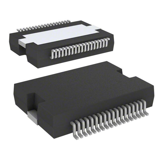
PowerSO36
ORDERING NUMBER: L9362
■
TYPICAL INTERNAL OSCILLATOR FREQUENCY 325kHZ
DESCRIPTION
The Quad Driver is an integrated quad low-side
power switch with power limitation, load interrupt
and shorted load detection, thermal shutdown, error detection via SPI interface and integrated Z-diodes for output clamping, free running diodes.
BLOCK DIAGRAM
VCC
VCC
ROL
VCC
=
=
Trigger
NON1
Reset
NON2
OUT1
dV/dt
Control
Driver
S
=
OUT2
R
OUT3
Overtemp.
NON3
NON1
OUT4
NON4
Reset
VCC
FR
RESET
I_SCB Filter
t_SCB
IRES
=
NON1
PGND1
PGND2
I_OL Filter
t_OL
=
SDI
Failure
Register
(FR)
VCC
=
CLK
=
Reset
≥1
=
VCC
OSC
=
Oscillator
NSC
Under
voltage
RESET
SDO
September 2013
CFB1
CFB2
IRES
99AT0007
PGND4
SCG Filter
t_SCG
Shift
Register
VCC
PGND3
=
NON1
LGND
SGND
RESET
CFB3
CFB4
NRES
1/17
�L9362
PIN CONNECTION
PGND1
N.C.
CFB1
OUT1
OUT1
CLK
NCS
N.C.
SGND
LGND
N.C.
SDO
SDI
OUT4
OUT4
CFB4
N.C.
PGND4
1
2
3
4
5
6
7
8
9
10
11
12
13
14
15
16
17
18
36
35
34
33
32
31
30
29
28
27
26
25
24
23
22
21
20
19
PGND2
N.C.
CFB2
OUT2
OUT2
NON1
NON2
N.C.
VCC
N.C.
NRES
NON3
NON4
OUT3
OUT3
CFB3
N.C.
PGND3
Frame connected to PGND
99AT0012
PIN FUNCTIONS
Pin No.
Pin Name
1
PGND1
Pin Description
Notes
Power Ground
2
N.C.
3
CFB1
Output Current feedback
4
OUT1
Output Power Switch
5
OUT1
6
CLK
Input Clock
Digital input, Schmitt trigger, internal Pullup current
7
NCS
inverted Chip Select Input
Digital input, Schmitt trigger, internal Pullup current
8
N.C.
Sinks current proportional to IOUT1
Output Power Switch
9
SGND
Signal Ground
10
LGND
Ground of digital part
11
N.C.
12
SDO
Serial Data Output
Digital tristate output
13
SDI
Serial Data Input
Digital input, Schmitt trigger, internal Pullup current
14
OUT4
Output Power Switch
15
OUT4
Output Power Switch
16
CFB4
Output Current feedback
17
N.C.
18
PGND4
Power Ground
19
PGND3
Power Ground
20
N.C.
21
CFB3
Output Current feedback
22
OUT3
Output Power Switch
23
OUT3
Output Power Switch
24
NON4
Inverted Control Signal Input
2/17
Sinks current proportional to IOUT4
Sinks current proportional to IOUT3
Digital input, Schmitt trigger, internal Pullup current
�L9362
PIN FUNCTIONS (continued)
Pin No.
Pin Name
25
NON3
Inverted Control Signal Input
Pin Description
Digital input, Schmitt trigger, internal Pullup current
Notes
26
NRES
Inverted Reset Input
Digital input, Schmitt trigger, internal Pullup current
27
N.C.
28
VCC
29
N.C.
30
NON2
Inverted Control Signal Input
Digital input, Schmitt trigger, internal Pullup current
31
NON1
Inverted Control Signal Input
Digital input, Schmitt trigger, internal Pullup current
32
OUT2
Output Power Switch
33
OUT2
Output Power Switch
34
CFB2
Output Current feedback
35
N.C.
36
PGND2
5V Supply Voltage Input
Sinks current proportional to IOUT2
Power Ground
THERMAL DATA
Symbol
Parameter
Test Conditions
Min.
Typ.
Max.
Unit
4.5
°C/W
Thermal resistance
Rth j-case
Thermal resistance junction to case
(one powerstage in use)
Die must be
soldered on the
frame.
Rthja
Thermal resistance junction-ambient
pad layout
50
°C/W
Rthja
Thermal resistance junction-ambient
pad layout + 6 cm2
on board heat sink
35
°C/W
ESD
ESD
2
MIL 883C
KV
ABSOLUTE MAXIMUM RATINGS
For externally applied voltages or currents exceeding these limits damage of the circuit may occur
Symbol
Parameter
Test Conditions
Min.
Typ.
Max.
Unit
-0.3
7
V
-0.3
45
V
3.0
A
-10
I_SCB
A
50
mJ
-0.3
7
V
-0.3
VCC
+0.3
V
-40
150
°C
Supply Voltages
Supply voltage
VCC
Outputs (Out 1 ... 4)
VOut
Continues output voltage
Ioutc
Continues current
ISCBpeak
WOFF
With no reverse
current.
Peak output current
Clamped energy at the switching OFF
For 2ms, see fig. 8
Inputs (NONx; NCS; CLK; NRES; SDI)
Input voltage
VIN
Outputs (SDO; CFB)
VOUT
Output voltage
Operating junction temperature
Tj
Note:
Operating junction temperature
The maximum ratings may not be exceeded under any circumstances, not even momentarily and individually, as permanent
damage to the IC will result.
3/17
�L9362
ELECTRICAL CHARACTERISTICS
4.5V VCC 5.5V, -40°C TJ 125°C, unless otherwise specified.
Symbol
Parameter
Test Conditions
Min.
Typ.
Max.
Unit
1.3
mA
17
mA
80
A
Supply current
ICCRES
Standby current
Without load.
Tj 85°C
NRES = LOW
ICCOPM
Operating mode
IOUT 1 ... 4 = 2A
Low voltage supply current
VCC < 0,5V
ICCLV
11
Inputs (NONx; NCS; CLK; NRES; SDI)
VINL
Low threshold
-0.3
0.2
VCC
V
VINH
High threshold
0.7
VCC
VCC
+0.3
V
Vhyst
Hysteresis
10
A
20
100
A
3
20
A
0.85
IIN
Input leakage current
VIN = VCC
IIN
Input current (NONx, NCS, CLK,
SDI)
VIN 0.8VCC
IIN NRES
Input current NRES
V
Serial Data Output
VSDOH
High output level
VSDOL
Low output level
(ISDO = 3.2mA)
ISDOL
Tristate leakage current
(NCS = HIGH;
VSDO = 0V ... VCC)
(ISDO = -2mA)
V
VCC
- 0.4
-10
0.4
V
10
A
10
A
Outputs (Out 1 ... 4)
IOUTL1
Leakage current 1
(NON = HIGH;
VOUT = 14V;
VCC = 5V)
Vclpa
Output clamp voltage
Vclpa (IOUT = 0.5A)
WOFF
Clamped energy at the switching
OFF 1)
For 2ms, see fig. 8
RDSON
ON resistance
IOUT = 2A; Tj = 150°C;
Tj = 25°C 2)
OVRp1
Positive output voltage ramp
(with inductive load)
OVRp2
OVRn
Negative output voltage ramp
45
VOUT = 30% ... 80% of
VBAT=16V 3)
VOUT =
VBAT ... 0.9 Vclp 3)
80% ... 30% of VBAT = 16V
with inductive load
0.3
50
60
V
50
mJ
250
500
300
m
m
0.9
1.35
V/s
2.25
V/s
0.75
0.3
0.9
1.35
V/s
3)
tdON
Turn ON delay
NON = 50%;
VOUT = 0.8 VBAT
0
4
10
s
tdOFF
Turn OFF delay
NON = 50%;
VOUT = 0.3 VBAT
0
4
10
s
Note 1:
Note 2:
Note 3:
4/17
Typical loads for the zener clamping and the output voltage ramps are:
a) 10, 16mH at all outputs or
b) 25, 160mH
At 150°C guaranteed by design and electrical characterisation
Tested with resistive load of Rload = 50
�L9362
ELECTRICAL CHARACTERISTICS (continued)
4.5V VCC 5.5V, -40°C TJ 125°C, unless otherwise specified.
Symbol
Parameter
Test Conditions
Min.
Typ.
Max.
Unit
5.0
A
Powerstage protection
ISCB
Short current detection and switch
off threshold
t_SCB
Short circuit switch off delay time
Vccmin
VCC undervoltage
With filter-time t_SCB.
3.0
30
s
4.0
V
1.65
2
mA/A
3
6
%
3
3.0
Current feedback
TRatio 1
ICFB / IOUT for IOUT=0.4...2A 4)
VCFB 1.8V
1.45
TMPS1 6)
5)
Temperature stability
for 0.4A to < 2.0A, related to
25°C
CURS1
for IOUT = 0.4A to 2A 5)
Current stability
gain/Gain at 2A
CURlin1 6)
CURlin2
Note 4:
Note 5:
Note 6:
for IOUT = 0.4A to 1.0A
for IOUT = 1.0A to 2.0A
4)
4)
TJ = -40°C
-12
17
%
TJ = +25°C
-6
10
%
TJ = +125°C
-5
5
%
1
0.7
%
%
0.390
VCC
0.435
VCC
V
0.2
Linearity Error
(within the calibration points
at 0.5A, 1A, 2A)
At 150°C guaranteed by design and electrical characterisation
Guaranteed by design and electrical characterisation
Values for TMPS1, CURlin1 and CURlin2 are typical values from testing results
Diagnostic
for IOUT 2A
VREF1
Short to GND threshold voltage
t_SCG
Short to GND filter time
140
250
s
Open load threshold current
10
55
mA
t_OL
Open load filter time
140
265
s
ROL
Pullup resistor at OUT1, OUT2,
OUT3 and OUT4 for OL detection
2.0
8.0
k
Temperature detection threshold 7)
155
190
°C
IOL
TOFF
Note 7:
170
Guaranteed by measurement and correlation
5/17
�L9362
ELECTRICAL CHARACTERISTICS (continued)
4.5V VCC 5.5V, -40°C TJ 125°C, unless otherwise specified.
Symbol
Parameter
Test Conditions
Min.
Typ.
Max.
Unit
3
MHz
Serial diagnostic link (external Load capacitor at SDO = 100pF)
fclk
Clock frequency
tclh
Minimum time CLK = HIGH
100
tcll
Minimum time CLK = LOW
100
tpcld
Propagation delay
50% duty cycle.
0
CLK to data at SDO valid.
tcsdv
NCS = LOW
To data at SDO valid.
tsclch
CLK low before NCS low
Setup time CLK to NCS
change H/L.
thclcl
CLK change L/H after
NCS = LOW
tscld
SDI input setup time
thcld
SDI input hold time
ns
ns
100
100
ns
ns
100
ns
100
ns
CLK change H/L after SDI
data valid.
20
ns
SDI data hold after CLK
change H/L.
20
ns
tsclcl
CLK low before NCS high
150
ns
thclch
CLK high after NCS high
150
ns
tpchdz
NCS L/H to output data float
tfNCS
NCS filter-time
Note: 8.
6/17
Pulses tfNCS will be
ignored.
10
100
ns
40
ns
Input Pin Capacitance of SDI, CLK, NCS, NON1, NON2, NON3, NON4 6pF typical; Output Pin Capacitance of SDO 12pF typica
�L9362
1.0 Diagnostic Register and SPI timing
Figure 1. Impulse diagram to read the Diagnostic Register
NCS
CLK
SDO
FSL
LSB
SDI
D2
D1
LSB
D1
D3
D2
D4
D3
D5
D4
D6
D5
MSB
D6
MSB
FR_RESET
99AT0008
Note: FR_RESET means Reset failure storage (internal signal)
Figure 2. Diagnostic Failure Register Structure
MSB
D7
LSB
D6
D5
D4
D3
D2
D1
D0
FSL
Failure indicator bit
(only valid during NCS = LOW
to the first L to H CLK change
1: failure stored
0: no failures
Status channel 4
D0 D1 Status
1 1 no failures
1 0 open circuit, channel on
0 1 short to battery or overtemperature
0 0 short to gnd, channel off
Status channel 3
D2 D3 corresponding to D0 D1
Status channel 2
D4 D5 corresponding to D0 D1
99AT0009/A
Status channel 1
D6 D7 corresponding to D0 D1
7/17
�L9362
Figure 3. Timing of the Serial Interface
NCS
tsclch
thclch
tcll
tclh
thclcl
tsclcl
CLK
tcsdv
SDO
tpcld
tpchdz
FSL
D0
tscld
SDI
D7
thcld
D0
D1
D7
99AT0010
Figure 4. Short-Circuit to GND Failure (SCG-Failure) Detection
Failure-detection time
for a SCG-failure
OFF
NON
ON
SCG-failure
Vdrain
Vref
Vdrain < Vref
at OFF-state
t_SCG (filter-time)
Filter-time
Failure-detection
Failure-store
00AT0002
8/17
�L9362
Figure 5. Open-Load Failure (OL-Failure) Detection
Sporadical failure-detection
Statical failure-detection
Failure detection active
for a sporadical OL-failure
NON
OFF
ON
Lload
I_OL
Lload > I_OL
Lload > I_OL
for t > t_OL
Diagnostic active
t_OL (filter-time)
Retrigger
t filter
Retrigger
filter
t_OL
t < t_OL
Sporadical
failure-detection
Failure-detection
Failure-store
00AT0003
9/17
�L9362
Figure 6. Different cases for an Open Load failure detection (case 1 to 10)
IOL = OL filter time
t OL
CASE 1
Non Input
Failure Register
Status
CASE 2
Non Input
Failure Register
Reset
Output
Current
IOL
t OL
Failure Register
Status
CASE 3
Output
Current
t OL
IOL
Failure Register
Status
CASE 4
Output
Current
t OL
IOL
t OL
Failure Register
Status
CASE 5
Output
Current
t OL
IOL
t OL
Failure Register
Status
CASE 6
Output
Current
IOL
t OL
t OL
Failure Register
Status
CASE 7
Output
Current
IOL
t OL
t OL
Failure Register
Status
CASE 8
Output
Current
t OL
t OL
Failure Register
Status
CASE 9
Output
Current
IOL
IOL
Failure Register
Status
00AT0004
10/17
t OL
t OL
t OL
Failure Register
Status
CASE 10
Output
Current
t OL
IOL
t OL
t OL
t OL
�L9362
Figure 7. Different cases for an Open Load failure detection (case 11 to 20)
CASE 11
Output
Current
IOL
t OL
t OL
Failure Register
Status
CASE 12
Output
Current
t OL
IOL
t OL
Failure Register
Status
CASE 13
Output
Current
t OL
t OL
t OL
t OL
IOL
Failure Register
Status
CASE 14
Output
Current
IOL
t OL
Failure Register
Status
CASE 15
Output
Current
t OL
t OL
IOL
t OL
Failure Register
Status
CASE 16
Output
Current
IOL
t OL
t OL
Failure Register
Status
CASE 17
Output
Current
t OL
t OL
IOL
Failure Register
Status
CASE 18
Output
Current
t OL
t OL
t OL
IOL
Failure Register
Status
CASE 19
Output
Current
t OL
t OL
IOL
Failure Register
Status
CASE 20
Non Input
Failure Register
Reset
Output
Current
t OL
t OL
t OL
t OL
IOL
Failure Register
Status
t OL
00AT0005
11/17
�L9362
Figure 8. Max Clamp Energy Specification
1000
Temp=25˚C
Temp=150˚C
Energy/[mJ]
800
600
400
200
0
0.0
2.0
4.0
6.0
Pulse width/[ms]
8.0
10.0
Figure 9. Tratio of Current Feedback output versus output current
1.80e-03
1.75e-03
1.70e-03
1.65e-03
Tratio
1.60e-03
Temp=-40˚C
Temp=-20˚C
Temp=25˚C
Temp=70˚C
Temp=150˚C
1.55e-03
1.50e-03
1.45e-03
1.40e-03
1.35e-03
1.30e-03
0.0
12/17
0.2
0.4
0.6
0.8 1.0 1.2
IOUT/[A]
1.4
1.6
1.8
2.0
�L9362
Figure 10. TMPS1 vs. Temperature (4.5V Vcc 5.5V; 0.5A Iout1...4 3A).
3
TMPS1/[%]
2
1
0
-1
-2
-3
-50
0
50
100
Temp./[˚C]
150
200
FUNCTIONAL DESCRIPTION
Introduction
The Quad Low Side Driver UF07 is built up of four identical channels (Low Side Drivers), controlled by four
CMOS input stages. Each Channel is protected against short to VBat and by a zener clamp against overvoltage.
A diagnostic logic recognizes four failure types at the output stage: overcurrent, short to GND, open-load and
overtemperature.
The failures are stored individually for each channel in one byte which can be read out via a serial interface (SPI).
Each channel has a current feedback output which sinks a current proportional to the load current of the Low
Side Switch.
Output Stage Control
Each of the four output stages is switched ON and OFF by an individual control line (NON-Input). The logic level of
the control line is CMOS compatible. The output transistors are switched off when the inputs are not connected.
Power Transistors
Each of the four output stages has its own zener clamp. This causes a voltage limitation at the power transistors
when inductive loads are switched off. Output voltage ramp occurring when the output is switched on or off, is
within defined limits. Output transistors can be connected in parallel to increase the current capability. In this
case, the associated inputs, outputs and current feedback outputs should be connected together.
Diagnostics
Following failures at the output stage are recognized:
Short circuit to VBat or overtemp................= SCB (Highest priority)
Short circuit to GND...................................=SCG
Open Load.................................................= OL (Lowest Priority)
13/17
�L9362
Short-Circuit and Overtemperature Protection (SCB)
If the output current increases above the short current limit for a longer time than t_SCB or if the temperature
increases above TOFF, then the power transistor is immediately switched off. It remains switched off until the
control signal at the NON-Input is switched off and on again. This filter time has the purpose to suppress wrong
detection on short spikes.
All four outputs have an independent overtemperature detection and shutdown. This measurement is active
while the powerstage is switched on.
The Short circuit detection and the overtemperature detection are using the same bit in the Diagnostic (one for
each channel).
A SCG failure will be recognized, when the drain voltage of the output stage is lower as the “Short Cut to Ground
threshold voltage”, while the output stage is switched off (see Fig. 4). The SCG failure is filtered with a digital
filter (t_SCG) to suppress the storage of a failure at small SCG spikes, which are typical during the transition of
the power output. This filter is triggered by the NON input and the (analog) SCG detection.
If the current through the output stage is lower than the IOL-reference, then an OL failure will be recognized
after a filter time. This measurement is active while the powerstage is switched on.
The Open Load failure detection has 2 different modes, the statical failure detection and the sporadic failure
detection. One main difference is, that a statical failure is transferred to the Failure register with the next rising
edge of NON, whereas a sporadic failure is transferred immediately to the Failure register (see fig. 5, 6 and 7).
In both failure modes the OL detection is filtered (t_OL=tOL) and is using together with the SCG detection the
same digital filter for suppression of spikes.
The failures are stored regarding to their priority (see above). A failure with a higher priority overwrites an eventually already detected failure with a lower priority.
Diagnostic interface
The communication between the microprocessor and the failure register runs via the SPI link. If there is a failure
stored in the failure register, the first bit of the shift register is set to a high level. With the H/L change at the NCS
pin the first bit of the diagnostic shift register will be transmitted to the SDO output. The SDO output is the serial
output from the diagnostic shift register and it is tristate when the NCS pin is high. The CLK pin clocks the diagnostic shift register. New SDO data will appear on every rising edge of the CLK pin and new SDI data will be
latched on every falling edge into the shift register. With the first positive pulse of the CLK the contents of the
failure register is copied to the SPI shift register and a internal reset (FR_RESET) is generated. This internal
reset clears the failure register and thus the failure register is capable of detecting failures also during the SPI
read cycle. There is no bus collision at a small spike at the NCS. The CLK has to be LOW, while the NCS signal
is changing.
Current feedback
Each channel has a current feedback output which sinks a current proportional to the load current of the Low
Side Switch. Using this output servo loop applications can be realized by applying a PWM signal to the NON
input. A typical diagram of the Current Feedback output at different temperatures is shown in figure 9.
14/17
�L9362
Reset
There are two different reset functions realized:
Undervoltage reset
As long as the voltage of Vcc is lower than Vccmin, the powerstages are switched off, the failure register
is reset and the SDO output remains tristate.
External reset
As long as the NRES pin is low following circuits are reset:
Powerstages
Failure register
and the SDO output is tristate.
Undervoltage protection
At Vcc below Vccmin the device remains switched off even if there is a voltage ramp at the OUT pin.
Figure 11. Application Circuit
VCC
C2
C1
VS
VCC
VCC
ROL
VCC
=
NON1
NON2
dV/dt
Control
Driver
S
Reset
OUT1
=
Trigger
(optional
for all
channels)
C1
OUT2
=
R
C2
OUT3
NON3
Overtemp.
NON1
C3
OUT4
NON4
Reset
μC
FR
RESET
C4
I_SCB Filter
t_SCB
IRES
=
NON1
VCC
PGND1
PGND2
I_OL Filter
t_OL
=
SDI
Failure
Register
(FR)
VCC
=
NON1
=
PGND4
SCG Filter
t_SCG
CLK
VCC
PGND3
Shift
Register
VCC
=
Reset
≥1
CFB1
=
VCC
NSC
OSC
CFB2
IRES
Under
voltage
RESET
SDO
LGND
SGND
CFB3
RESET
=
Oscillator
ADC
CFB4
NRES
99AT0011
15/17
�L9362
DIM.
mm
MIN.
TYP.
A
a1
inch
MAX.
MIN.
TYP.
3.60
0.10
0.30
a2
MAX.
0.1417
0.0039
0.0118
3.30
0.1299
a3
0
0.10
b
0.22
0.38
0.0087
0.0150
c
0.23
0.32
0.0091
0.0126
D
15.80
16.00 0.6220
0.6299
D1
9.40
9.80
0.3701
E
13.90
14.5
0.5472
0.5709
E1
10.90
11.10 0.4291
0.4370
E2
E3
e
6.20
0.3858
0.1142
0.2283
0.65
e3
0
H
15.50
h
0.4350
0.10
0.0039
15.90 0.6102
1.10
0.8
0.2441
0.0256
11.05
G
L
0.0039
2.90
5.80
OUTLINE AND
MECHANICAL DATA
1.10
0.6260
0.0433
0.0315
N
10˚ (max)
s
8˚ (max)
0.0433
PowerSO-36
Note: “D and E1” do not include mold flash or protusions.
- Mold flash or protusions shall not exceed 0.15mm (0.006”)
- Critical dimensions are "a3", "E" and "G".
0096119 C
16/17
�L9362
Please Read Carefully:
Information in this document is provided solely in connection with ST products. STMicroelectronics NV and its subsidiaries (“ST”) reserve the
right to make changes, corrections, modifications or improvements, to this document, and the products and services described herein at any
time, without notice.
All ST products are sold pursuant to ST’s terms and conditions of sale.
Purchasers are solely responsible for the choice, selection and use of the ST products and services described herein, and ST assumes no
liability whatsoever relating to the choice, selection or use of the ST products and services described herein.
No license, express or implied, by estoppel or otherwise, to any intellectual property rights is granted under this document. If any part of this
document refers to any third party products or services it shall not be deemed a license grant by ST for the use of such third party products
or services, or any intellectual property contained therein or considered as a warranty covering the use in any manner whatsoever of such
third party products or services or any intellectual property contained therein.
UNLESS OTHERWISE SET FORTH IN ST’S TERMS AND CONDITIONS OF SALE ST DISCLAIMS ANY EXPRESS OR IMPLIED
WARRANTY WITH RESPECT TO THE USE AND/OR SALE OF ST PRODUCTS INCLUDING WITHOUT LIMITATION IMPLIED
WARRANTIES OF MERCHANTABILITY, FITNESS FOR A PARTICULAR PURPOSE (AND THEIR EQUIVALENTS UNDER THE LAWS
OF ANY JURISDICTION), OR INFRINGEMENT OF ANY PATENT, COPYRIGHT OR OTHER INTELLECTUAL PROPERTY RIGHT.
ST PRODUCTS ARE NOT DESIGNED OR AUTHORIZED FOR USE IN: (A) SAFETY CRITICAL APPLICATIONS SUCH AS LIFE
SUPPORTING, ACTIVE IMPLANTED DEVICES OR SYSTEMS WITH PRODUCT FUNCTIONAL SAFETY REQUIREMENTS; (B)
AERONAUTIC APPLICATIONS; (C) AUTOMOTIVE APPLICATIONS OR ENVIRONMENTS, AND/OR (D) AEROSPACE APPLICATIONS
OR ENVIRONMENTS. WHERE ST PRODUCTS ARE NOT DESIGNED FOR SUCH USE, THE PURCHASER SHALL USE PRODUCTS
AT PURCHASER’S SOLE RISK, EVEN IF ST HAS BEEN INFORMED IN WRITING OF SUCH USAGE, UNLESS A PRODUCT IS
EXPRESSLY DESIGNATED BY ST AS BEING INTENDED FOR “AUTOMOTIVE, AUTOMOTIVE SAFETY OR MEDICAL” INDUSTRY
DOMAINS ACCORDING TO ST PRODUCT DESIGN SPECIFICATIONS. PRODUCTS FORMALLY ESCC, QML OR JAN QUALIFIED ARE
DEEMED SUITABLE FOR USE IN AEROSPACE BY THE CORRESPONDING GOVERNMENTAL AGENCY.
Resale of ST products with provisions different from the statements and/or technical features set forth in this document shall immediately void
any warranty granted by ST for the ST product or service described herein and shall not create or extend in any manner whatsoever, any
liability of ST.
ST and the ST logo are trademarks or registered trademarks of ST in various countries.
Information in this document supersedes and replaces all information previously supplied.
The ST logo is a registered trademark of STMicroelectronics. All other names are the property of their respective owners.
© 2013 STMicroelectronics - All rights reserved
STMicroelectronics group of companies
Australia - Belgium - Brazil - Canada - China - Czech Republic - Finland - France - Germany - Hong Kong - India - Israel - Italy - Japan Malaysia - Malta - Morocco - Philippines - Singapore - Spain - Sweden - Switzerland - United Kingdom - United States of America
www.st.com
DocID7708 Rev 4
17/17
�