L9663
Automotive PSI5 Transceiver IC
Datasheet - production data
Short to ground tolerant with ±1.5 V ground
shift
32-bit SPI interface with address multiplexing
Operating voltage: VB = 4.8 V (5.2 V for sync
pulses with 3.5 V step) to 35 V
Ambient temperature range: -40°C to 140 °C
Package: VFQFPN28 or TQFP32EP
*$3*����������36
*$'*����������36
VFQFPN28
TQFP32
(Exposed pad down)
Description
The Peripheral Sensor Interface (PSI5) is an
interface for automotive sensor applications. PSI5
is an open standard based on existing sensor
interfaces for peripheral sensors and offers a
universal and flexible solution for multiple sensor
applications.
Features
AEC-Q100 qualified
2-channel PSI5 transceiver compatible with
rev. 1.3 and rev. 2.x
The PSI5 interface allows asynchronous or
synchronous operations and different bus modes.
The device is compatible with both v1.3 and v2.x
PSI5 revisions (limitations are specified inside this
document). It operates with a wide range of
sensor supply current and variable data word
length (8 to 28 bit).
Manchester coded digital data transmission
High data transmission speed of 125 kbps
(optional 83.3 kbps and 189 kbps)
High EMC robustness and low emission
Bootstrap circuits for sync pulses
Current limitation and voltage clamp on
interface pins
Integrated charge pump stage for preregulation with spread spectrum approach
Integrated FLL module for high accuracy timing
control
Reverse voltage protection structure
The sensors are connected to the ECU using the
same line for power supply and data
transmission. The transceiver IC provides a preregulated voltage to the sensors and reads in the
transmitted sensor data.
The PSI5 interface allows either point to point
connection or bussed mode.
Table 1. Device summary
Order code
L9663
L9663-TR
L9663-1
L9663-TR-1
July 2019
This is information on a product in full production.
Package
TQFP32 (Exposed pad)
VFQFPN28
DS11401 Rev 5
Packing
Tray
Tape & Reel
Tray
Tape & Reel
1/105
www.st.com
�Contents
L9663
Contents
1
2
3
2/105
Overall description . . . . . . . . . . . . . . . . . . . . . . . . . . . . . . . . . . . . . . . . . . 6
1.1
Simplified block diagram . . . . . . . . . . . . . . . . . . . . . . . . . . . . . . . . . . . . . . 6
1.2
Main functionality . . . . . . . . . . . . . . . . . . . . . . . . . . . . . . . . . . . . . . . . . . . . 7
1.3
VQFPN28 pins description . . . . . . . . . . . . . . . . . . . . . . . . . . . . . . . . . . . . . 9
1.4
TQFP32 pins description . . . . . . . . . . . . . . . . . . . . . . . . . . . . . . . . . . . . . .11
1.5
Maximum ratings . . . . . . . . . . . . . . . . . . . . . . . . . . . . . . . . . . . . . . . . . . . 13
1.6
Detailed block diagram . . . . . . . . . . . . . . . . . . . . . . . . . . . . . . . . . . . . . . . 14
1.7
Power up sequence . . . . . . . . . . . . . . . . . . . . . . . . . . . . . . . . . . . . . . . . . 16
Power supply . . . . . . . . . . . . . . . . . . . . . . . . . . . . . . . . . . . . . . . . . . . . . . 17
2.1
Internal supply . . . . . . . . . . . . . . . . . . . . . . . . . . . . . . . . . . . . . . . . . . . . . 17
2.2
VAS supply and pre-regulator . . . . . . . . . . . . . . . . . . . . . . . . . . . . . . . . . . 18
2.3
Voltage supply for synchronous pulse generation VSYNCx
2.4
Power supply for PSI5 sensor line . . . . . . . . . . . . . . . . . . . . . . . . . . . . . . 20
2.5
Frequency references . . . . . . . . . . . . . . . . . . . . . . . . . . . . . . . . . . . . . . . 22
2.6
Reset handling . . . . . . . . . . . . . . . . . . . . . . . . . . . . . . . . . . . . . . . . . . . . . 24
. . . . . . . . . . . . . . . . 19
Satellite interface . . . . . . . . . . . . . . . . . . . . . . . . . . . . . . . . . . . . . . . . . . . 25
3.1
Receiver with digital sampling and filtering . . . . . . . . . . . . . . . . . . . . . . . 25
3.2
Manchester decoder and error detection . . . . . . . . . . . . . . . . . . . . . . . . . 26
3.3
Receive block . . . . . . . . . . . . . . . . . . . . . . . . . . . . . . . . . . . . . . . . . . . . . . 26
3.3.1
PSI5 receive register . . . . . . . . . . . . . . . . . . . . . . . . . . . . . . . . . . . . . . . 27
3.3.2
Sensor data buffer . . . . . . . . . . . . . . . . . . . . . . . . . . . . . . . . . . . . . . . . . 30
3.3.3
Interrupt generator . . . . . . . . . . . . . . . . . . . . . . . . . . . . . . . . . . . . . . . . . 33
3.3.4
Automatic storage of sensor initialization data . . . . . . . . . . . . . . . . . . . 33
3.4
Upstream data buffer . . . . . . . . . . . . . . . . . . . . . . . . . . . . . . . . . . . . . . . . 35
3.5
Trigger pulse generator for synchronous pulses . . . . . . . . . . . . . . . . . . . 36
3.6
Synchronous pulse generator . . . . . . . . . . . . . . . . . . . . . . . . . . . . . . . . . 37
3.7
Safety concepts . . . . . . . . . . . . . . . . . . . . . . . . . . . . . . . . . . . . . . . . . . . . 38
3.7.1
Voltage monitoring check . . . . . . . . . . . . . . . . . . . . . . . . . . . . . . . . . . . . 38
3.7.2
Sensor data consistency . . . . . . . . . . . . . . . . . . . . . . . . . . . . . . . . . . . . 38
3.7.3
Buffer empty check . . . . . . . . . . . . . . . . . . . . . . . . . . . . . . . . . . . . . . . . 39
DS11401 Rev 5
�L9663
4
5
Contents
DOUTx path check . . . . . . . . . . . . . . . . . . . . . . . . . . . . . . . . . . . . . . . . 39
3.7.5
Cross coupling test . . . . . . . . . . . . . . . . . . . . . . . . . . . . . . . . . . . . . . . . 40
Diagnosis . . . . . . . . . . . . . . . . . . . . . . . . . . . . . . . . . . . . . . . . . . . . . . . . . 42
4.1
PSIx output voltage clamping circuit . . . . . . . . . . . . . . . . . . . . . . . . . . . . 42
4.2
PSIx output under voltage monitoring . . . . . . . . . . . . . . . . . . . . . . . . . . . 42
4.3
PSIx short circuit detection . . . . . . . . . . . . . . . . . . . . . . . . . . . . . . . . . . . . 43
4.4
PSIx reverse voltage monitoring . . . . . . . . . . . . . . . . . . . . . . . . . . . . . . . 44
4.5
VAS under/over voltage monitoring . . . . . . . . . . . . . . . . . . . . . . . . . . . . . . 44
4.6
Monitoring of Synchronous Pulse amplitude . . . . . . . . . . . . . . . . . . . . . . 45
Communication interface . . . . . . . . . . . . . . . . . . . . . . . . . . . . . . . . . . . . 47
5.1
Device registers . . . . . . . . . . . . . . . . . . . . . . . . . . . . . . . . . . . . . . . . . . . . 47
5.2
SPI interface . . . . . . . . . . . . . . . . . . . . . . . . . . . . . . . . . . . . . . . . . . . . . . . 82
5.3
6
3.7.4
5.2.1
Physical layer and signal description . . . . . . . . . . . . . . . . . . . . . . . . . . . 82
5.2.2
Clock and data characteristics . . . . . . . . . . . . . . . . . . . . . . . . . . . . . . . . 83
5.2.3
Frame definition . . . . . . . . . . . . . . . . . . . . . . . . . . . . . . . . . . . . . . . . . . . 84
5.2.4
Communication frames . . . . . . . . . . . . . . . . . . . . . . . . . . . . . . . . . . . . . 84
Direct interface . . . . . . . . . . . . . . . . . . . . . . . . . . . . . . . . . . . . . . . . . . . . . 87
Electrical characteristics . . . . . . . . . . . . . . . . . . . . . . . . . . . . . . . . . . . . 88
6.1
SPI interface . . . . . . . . . . . . . . . . . . . . . . . . . . . . . . . . . . . . . . . . . . . . . . . 96
7
Errata . . . . . . . . . . . . . . . . . . . . . . . . . . . . . . . . . . . . . . . . . . . . . . . . . . . . 99
8
Package information . . . . . . . . . . . . . . . . . . . . . . . . . . . . . . . . . . . . . . . 100
9
8.1
TQFP32 (7x7x1.0 mm exp. pad down) package information . . . . . . . . . 100
8.2
VFQFPN-28 (5x5x1.0 mm) package information . . . . . . . . . . . . . . . . . . 102
Revision history . . . . . . . . . . . . . . . . . . . . . . . . . . . . . . . . . . . . . . . . . . 104
DS11401 Rev 5
3/105
3
�List of tables
L9663
List of tables
Table 1.
Table 2.
Table 3.
Table 4.
Table 5.
Table 6.
Table 7.
Table 8.
Table 9.
Table 10.
Table 11.
Table 12.
Table 13.
Table 14.
Table 15.
Table 16.
Table 17.
Table 18.
Table 19.
Table 20.
Table 21.
Table 22.
Table 23.
Table 24.
Table 25.
Table 26.
Table 27.
Table 28.
Table 29.
Table 30.
4/105
Device summary . . . . . . . . . . . . . . . . . . . . . . . . . . . . . . . . . . . . . . . . . . . . . . . . . . . . . . . . . . 1
VQFPN28 pin-out . . . . . . . . . . . . . . . . . . . . . . . . . . . . . . . . . . . . . . . . . . . . . . . . . . . . . . . . . 9
TQFP32 pin-out . . . . . . . . . . . . . . . . . . . . . . . . . . . . . . . . . . . . . . . . . . . . . . . . . . . . . . . . . 11
Pin maximum ratings . . . . . . . . . . . . . . . . . . . . . . . . . . . . . . . . . . . . . . . . . . . . . . . . . . . . . 13
Time (t0-t2) vs SensorData. . . . . . . . . . . . . . . . . . . . . . . . . . . . . . . . . . . . . . . . . . . . . . . . . 30
Error codes in sensor communication . . . . . . . . . . . . . . . . . . . . . . . . . . . . . . . . . . . . . . . . 31
Faults priority . . . . . . . . . . . . . . . . . . . . . . . . . . . . . . . . . . . . . . . . . . . . . . . . . . . . . . . . . . . 31
Time (t0-t7) vs SensorData. . . . . . . . . . . . . . . . . . . . . . . . . . . . . . . . . . . . . . . . . . . . . . . . . 32
Doutx test mode bit value . . . . . . . . . . . . . . . . . . . . . . . . . . . . . . . . . . . . . . . . . . . . . . . . . . 39
Operating conditions . . . . . . . . . . . . . . . . . . . . . . . . . . . . . . . . . . . . . . . . . . . . . . . . . . . . . . 88
VINTx internal supply . . . . . . . . . . . . . . . . . . . . . . . . . . . . . . . . . . . . . . . . . . . . . . . . . . . . . 88
VAS supply . . . . . . . . . . . . . . . . . . . . . . . . . . . . . . . . . . . . . . . . . . . . . . . . . . . . . . . . . . . . . 89
VAS external MOS. . . . . . . . . . . . . . . . . . . . . . . . . . . . . . . . . . . . . . . . . . . . . . . . . . . . . . . . 89
VAS pre regulator . . . . . . . . . . . . . . . . . . . . . . . . . . . . . . . . . . . . . . . . . . . . . . . . . . . . . . . . 90
VSYNCx . . . . . . . . . . . . . . . . . . . . . . . . . . . . . . . . . . . . . . . . . . . . . . . . . . . . . . . . . . . . . . . . . . . . . . . . . . . . . . . . . 91
PSI5 output supply . . . . . . . . . . . . . . . . . . . . . . . . . . . . . . . . . . . . . . . . . . . . . . . . . . . . . . . 91
PSI5 receiver . . . . . . . . . . . . . . . . . . . . . . . . . . . . . . . . . . . . . . . . . . . . . . . . . . . . . . . . . . . 92
Sync generator . . . . . . . . . . . . . . . . . . . . . . . . . . . . . . . . . . . . . . . . . . . . . . . . . . . . . . . . . . 93
Reset . . . . . . . . . . . . . . . . . . . . . . . . . . . . . . . . . . . . . . . . . . . . . . . . . . . . . . . . . . . . . . . . . 94
VAS under/over voltage monitoring. . . . . . . . . . . . . . . . . . . . . . . . . . . . . . . . . . . . . . . . . . . 94
Synchronous pulse amplitude monitoring . . . . . . . . . . . . . . . . . . . . . . . . . . . . . . . . . . . . . . 95
Time slot monitoring . . . . . . . . . . . . . . . . . . . . . . . . . . . . . . . . . . . . . . . . . . . . . . . . . . . . . . 95
Digital I/O . . . . . . . . . . . . . . . . . . . . . . . . . . . . . . . . . . . . . . . . . . . . . . . . . . . . . . . . . . . . . . 95
Frequency references . . . . . . . . . . . . . . . . . . . . . . . . . . . . . . . . . . . . . . . . . . . . . . . . . . . . . 95
SPI communication timing . . . . . . . . . . . . . . . . . . . . . . . . . . . . . . . . . . . . . . . . . . . . . . . . . 97
Direct interface . . . . . . . . . . . . . . . . . . . . . . . . . . . . . . . . . . . . . . . . . . . . . . . . . . . . . . . . . . 97
Errata . . . . . . . . . . . . . . . . . . . . . . . . . . . . . . . . . . . . . . . . . . . . . . . . . . . . . . . . . . . . . . . . . 99
TQFP32 (7x7x1.0 mm exp. pad down) package mechanical data . . . . . . . . . . . . . . . . . . 101
VFQFPN-28 (5x5x1.0 mm) package mechanical data . . . . . . . . . . . . . . . . . . . . . . . . . . . 102
Document revision history . . . . . . . . . . . . . . . . . . . . . . . . . . . . . . . . . . . . . . . . . . . . . . . . 104
DS11401 Rev 5
�L9663
List of figures
List of figures
Figure 1.
Figure 2.
Figure 3.
Figure 4.
Figure 5.
Figure 6.
Figure 7.
Figure 8.
Figure 9.
Figure 10.
Figure 11.
Figure 12.
Figure 13.
Figure 14.
Figure 15.
Figure 16.
Figure 17.
Figure 18.
Figure 19.
Figure 20.
Figure 21.
Figure 22.
Figure 23.
Figure 24.
Figure 25.
Figure 26.
Figure 27.
Figure 28.
Figure 29.
Figure 30.
Figure 31.
Figure 32.
Figure 33.
Simplified block diagram . . . . . . . . . . . . . . . . . . . . . . . . . . . . . . . . . . . . . . . . . . . . . . . . . . . . 6
VQFPN28 pins connection diagram (top view) . . . . . . . . . . . . . . . . . . . . . . . . . . . . . . . . . . . 9
TQFP32 pins connection diagram (top view) . . . . . . . . . . . . . . . . . . . . . . . . . . . . . . . . . . . 11
Detailed block diagram . . . . . . . . . . . . . . . . . . . . . . . . . . . . . . . . . . . . . . . . . . . . . . . . . . . . 14
Supply line model for PSI5 . . . . . . . . . . . . . . . . . . . . . . . . . . . . . . . . . . . . . . . . . . . . . . . . . 15
Power-up sequence of transceiver IC. . . . . . . . . . . . . . . . . . . . . . . . . . . . . . . . . . . . . . . . . 16
Internal power supply and reset generation . . . . . . . . . . . . . . . . . . . . . . . . . . . . . . . . . . . . 17
Input structure of supply . . . . . . . . . . . . . . . . . . . . . . . . . . . . . . . . . . . . . . . . . . . . . . . . . . . 17
VAS application diagram . . . . . . . . . . . . . . . . . . . . . . . . . . . . . . . . . . . . . . . . . . . . . . . . . . . 19
Block diagram Transceiver 1 . . . . . . . . . . . . . . . . . . . . . . . . . . . . . . . . . . . . . . . . . . . . . . . 21
Internal oscillator vs external clock frequency . . . . . . . . . . . . . . . . . . . . . . . . . . . . . . . . . . 23
FLL clock error detection . . . . . . . . . . . . . . . . . . . . . . . . . . . . . . . . . . . . . . . . . . . . . . . . . . 23
Block diagram of incoming data buffer . . . . . . . . . . . . . . . . . . . . . . . . . . . . . . . . . . . . . . . . 27
PSI5 v1.3 frame . . . . . . . . . . . . . . . . . . . . . . . . . . . . . . . . . . . . . . . . . . . . . . . . . . . . . . . . . 28
PSI5 v2.0 frame . . . . . . . . . . . . . . . . . . . . . . . . . . . . . . . . . . . . . . . . . . . . . . . . . . . . . . . . . 28
Sensor buffer in synchronous mode diagram . . . . . . . . . . . . . . . . . . . . . . . . . . . . . . . . . . . 30
Sensor buffer in asynchronous mode diagram . . . . . . . . . . . . . . . . . . . . . . . . . . . . . . . . . . 32
Block diagram with interrupt pins . . . . . . . . . . . . . . . . . . . . . . . . . . . . . . . . . . . . . . . . . . . . 33
Timing diagram . . . . . . . . . . . . . . . . . . . . . . . . . . . . . . . . . . . . . . . . . . . . . . . . . . . . . . . . . . 34
ECU to sensor communication diagram . . . . . . . . . . . . . . . . . . . . . . . . . . . . . . . . . . . . . . . 35
Short (in case 1 µs < tw < 5 µs) Sync Pulse trigger, compliant to PSI5 standard . . . . . . . . 38
Timing for PSIx under voltage detection . . . . . . . . . . . . . . . . . . . . . . . . . . . . . . . . . . . . . . . 42
Timing for PSIx reverse voltage detection . . . . . . . . . . . . . . . . . . . . . . . . . . . . . . . . . . . . . 44
Timing for VAS under voltage detection . . . . . . . . . . . . . . . . . . . . . . . . . . . . . . . . . . . . . . . 44
Timing for sync pulse voltage monitoring . . . . . . . . . . . . . . . . . . . . . . . . . . . . . . . . . . . . . . 45
SPI interface . . . . . . . . . . . . . . . . . . . . . . . . . . . . . . . . . . . . . . . . . . . . . . . . . . . . . . . . . . . . 82
Operation on internal register (with upstream data buffer) . . . . . . . . . . . . . . . . . . . . . . . . . 85
Init data reading . . . . . . . . . . . . . . . . . . . . . . . . . . . . . . . . . . . . . . . . . . . . . . . . . . . . . . . . . 85
Sensor data reading . . . . . . . . . . . . . . . . . . . . . . . . . . . . . . . . . . . . . . . . . . . . . . . . . . . . . . 86
Sync generator . . . . . . . . . . . . . . . . . . . . . . . . . . . . . . . . . . . . . . . . . . . . . . . . . . . . . . . . . . 93
SPI communication timing diagram . . . . . . . . . . . . . . . . . . . . . . . . . . . . . . . . . . . . . . . . . . 96
TQFP32 (7x7x1.0 mm exp. pad down) package outline. . . . . . . . . . . . . . . . . . . . . . . . . . 100
VFQFPN-28 (5x5x1.0 mm) package outline . . . . . . . . . . . . . . . . . . . . . . . . . . . . . . . . . . . 102
DS11401 Rev 5
5/105
5
�Overall description
L9663
1
Overall description
1.1
Simplified block diagram
Figure 1. Simplified block diagram
6\QF�SXOVH�
VXSSO\
36,��,&
9DV�SUH�
UHJXODWRU
,QWHUQDO�VXSSO\
32:(5�6833/<
75$16&(,9(5��
2XWSXW�OLQH�YROWDJH�
PRQLWRULQJ
EDFN�WR�
EDFN
6\QFKURQRXV�
SXOVH�JHQHUDWRU
36,�
FXUUHQW�
OLPLWDWLRQ�
JDWH�
GULYHU
6�
5HFHLYHU
75$16&(,9(5��
36,�
6�
6�
6�
7HVW�ORJLF
5$0�UHJLVWHU
IRU�VHQVRU�GDWD
0DQFKHVWHU�
'HFRGHU
'LDJQRVLV
6\QF�SXOVH
WULJJHU
8SVWUHDP�
GDWD�EXIIHU
&RQILJXUDWLRQ�
UHJLVWHU�
',*,7$ /�6(&7,21
&20081,&$7,21�,17(5)$&(6
63,
,QWHUIDFH
'LUHFW�
,QWHUIDFH
5HVHW�&RQWURO
*$3*36�����
6/105
DS11401 Rev 5
�L9663
1.2
Overall description
Main functionality
The transceiver IC can be used in two different modes (Mode 1 or Mode 2)(a) . The system
configuration called Mode 1 performs the decoding effort of sensor signals in the IC. The
system configuration called Mode 2 is a front-end to a PSI5 decoder contained in an
external device (typically a µC with a dedicated module).
The transceiver IC can monitor all internally generated relevant voltages, such as VSYNCx
VAS and V_PSIx.
The PSI5 interfaces inside the IC are supplied by a separate input pin VAS. If only
asynchronous mode is required, the VAS voltage is sufficient for the sensor power supply.
When synchronous mode is required, a higher voltage than VAS is needed in order to
generate the synchronous pulses. This voltage VSYNCx is generated by a dedicated
bootstrap circuit for each channel.
For direct supply from battery, the transceiver IC includes a VAS pre-regulator supplied by
VASSUP-pin: the pre-regulator can drive an external FET to regulate the VAS voltage to
7.6 V or 5.3 V. In case of low voltage level at VASSUP, an integrated charge pump is
implemented, with supply from VASSUP.
The internal analog and digital circuits are supplied by VB. The external voltage on VDD pin
is used to supply the digital output pins; VDD pin can be used to switch the digital outputs
from 5 V output level (default) to 3.3 V output level.
The PSI5 transceiver is functional in the whole VDD, VB, VASSUP and VAS power supply
range.
The internal voltage supplies (VSYNCx) are automatically activated by the transceiver IC
depending on the operating mode whenever they are needed.
Each transceiver interface can be activated and deactivated by an SPI command. At startup, the interfaces are off by default.
The communication interface block includes two different interfaces. In mode 1, SPI is used
for data transfer. In mode 2, the direct interface is used. The data from and to the sensors
will be transmitted bit-wise between the transceiver IC and the µC. The data evaluation and
error handling for frame errors will be done in the PSI5 controller which is integrated in the
µC.
Transceiver 1 and 2 supply the sensors and generate the synchronous pulses for
synchronous data transfer (if required) from the sensors to the transceiver and for data
transfer from the ECU to the sensors.
A data transfer from the ECU to the sensors can be performed:
by using sync pulses with different duration (PSI5 2.x standard)
by masking of sync pulses (PSI5 1.3 and 2.x standard)
The sync pulse trigger can be generated by an SPI command, by a dedicated pin (for
connection to the Synchronous Pulse Output Block included in the microcontroller) or by an
integrated automatic timer.
a. Mode 1 and Mode 2 are two system architectures which relate on the way L9663 communicates with the
microcontroller. Depending on the chosen architecture, the µC must configure the IC with the correct setup.
DS11401 Rev 5
7/105
104
�Overall description
L9663
The Transceivers 1 and 2 limit the current and the PSIx voltage (PSI5-requirement when
VAS is too high because of failure in the VAS power supply, less than 11 V in data
transmission or less than 16.5 V in sync pulse).
The current modulated signal received from sensor is detected and digitally converted. This
sensor data will then either be:
8/105
First Manchester decoded by the Manchester Decoder block with mark space error
correction and then transferred to the "receive data buffer" module (Mode 1). The data
from the new sensor frames will be saved in a buffer and then will be transferred to the
µC via SPI.
Transferred directly to the µC (Mode 2). In this case the output of the transceiver is a
Manchester-coded signal without error correction that falls under microcontroller
responsibility.
DS11401 Rev 5
�L9663
VQFPN28 pins description
0,62
9''
'*1'
9,17'
70
5(6(71
&6
Figure 2. VQFPN28 pins connection diagram (top view)
��
��
��
��
��
��
��
��
026,
&/.,1
�
��
1&
6N��@
&�
&5&�/6%
'DWD�06%
'DWD�/6%
36,��)UDPH�S� ����������ELW
'DWD�5HJLRQ�
�N� �������������������ELW�
6�
6�
'�
'>N��@
'>N��@
&�
&�
&5&�RU�SDULW\
�����ELW
6WDUW�ELWV
��ELW
*$3*36�����
Figure 15. PSI5 v2.0 frame
6�
6�
6WDUW�ELWV
��ELW
28/105
'�
'�
'�
0�
0�
)�
0HVVDJLQJ
RSWLRQDO
�����ELW
)>T��@
)UDPH�FRQWURO
RSWLRQDO
��������������ELW
(�
(>U��@
6WDWXV
RSWLRQDO
�����RU���ELW
%�
%�
%>P��@
3D\ORDG�'DWD�5HJLRQ���
�RSWLRQDO�
P� ��«���ELW
�ELW�JUDQXODULW\
DS11401 Rev 5
$�
'>N��@
'>N��@ '>N��@
$>Q��@
$>Q��@
3D\ORDG�'DWD�5HJLRQ���
Q� ���«���ELW
�ELW�JUDQXODULW\
$>Q��@
&�
&5&�/6%
'DWD�5HJLRQ��N� ��������ELW�
&5&�06%
'DWD�06%
'DWD�/6%
36,��)UDPH�S� ����������ELW
&�
&�
&5&�RU�SDULW\
�����ELW
*$3*36�����
�L9663
Satellite interface
In case of PSI5 v2.x, the length of the data region can vary between k = 10 … 28 bits, with
1-bit granularity. The data region can be split into the following fields and regions:
Signal payload region 1 with data bits A0 … A[n-1] (scalable n = 10…24 with 1-bit
granularity)
Signal payload region 2 with data bits B0 … B[m-1] (scalable m = 0…12 with 1-bit
granularity)
Sensor status E0.. E[r-1] (optional r = 0, 1 or 2 bit)
–
Frame control, type of frame F0, …F[q-1] (optional q = 0, 1, 2, 3 or 4 bit)
–
This optional status bit can be used to show that the data of the current frame are
faulty.
This frame control can be used to number the frames which are sent after a sync
pulse.
Serial (slow) messaging channel (optional) M0, M1 (optional 0 or 2 bit)
Time slot monitoring
The time slot monitoring is active only in synchronous mode.
The time slot monitoring is required to check if the sensors connected to the transceiver
work properly in terms of timing, i.e. if they are sending data frames within their defined time
slot.
Basic features:
3 configurable modes
Failure bit
During a synchronous pulse period (TSYNC), a maximum number of 6 frames can be
configured. Each frame has its own time slot, to be configured through dedicated
configuration registers. The registers contain the reference time needed to check if the
sensor data is transmitted during the defined time slot.
The resolution of time slots is 1 µs. The time slot monitoring timings are applied starting
from the internal sync pulse trigger. This internal trigger falls td_SPI (or td_SYNC, depending
on sync pulse trigger configuration) after the external one (via SPI or SYNC pin).
Three different configurations for the time slot monitoring are available:
Standard configuration: monitoring the correct start and end time of a unique frame
within a time slot
Simple configuration: monitoring only the end time of a frame within a time slot
No monitoring configuration: monitoring is disabled and data are stored in successive
slots.
The time slot monitoring can be activated/deactivated separately for each interface
(registers CHx_CR1, bits TSMx_SEL).
In case of standard configuration, the IC accepts as valid frame in a timeslot only a frame
which starts and ends within its timeslot; if more than one valid frame is received within its
timeslot, only the last one received is kept.
On the other side, in case frames span across slots, the frame is discarded and the error
code 1FC (timing violation) is stored in the correspondent buffer; in this case the decoder is
reset at every slot start. After this reset if a frame was being decoded, a slot error is set in
the previous slot but no slot error is set. Then the Manchester FSM after reset checks again
DS11401 Rev 5
29/105
104
�Satellite interface
L9663
for two valid start bits and so a new incoming frame can be stored without error in the new
timeslot.
In the simple configuration, the last valid message which ends in a timeslot is stored in the
buffer of the slot (so if a frame is currently stored in a timeslot and an incoming frame ends
in this timeslot, the old data are overwritten). In this mode slot error is never set.
It is also possible to disable the time slot monitoring and in this case, no timing check is
done: the first frame is assigned to the first buffer, the second to the second, and so on. This
means that the buffer index is incremented every time a frame is received both valid and
invalid (Manchester communication error).
After reset, the default mode for the time slot monitoring is "monitoring disabled".
3.3.2
Sensor data buffer
To avoid loss of data, a data buffer for each PSI5 transceiver is necessary. While the data
buffer is being read by SPI, at the beginning of the sensor data transfer the data register is
cleared and a new data frame can be accepted.
The incoming PSI5 sensor data, together with CRC and SID/GBIT (if selected) are written
into a receive buffer, which is large enough to hold the data of one sync pulse cycle (i.e. up
to six sensors). In order to avoid data-mixing between different cycle times the data must be
fetched by the µC before the next transmission cycle starts.
The figure below shows how sensor buffers are updated in synchronous mode.
At t0 the buffers contain no data; then a sync pulse is sent and data are received and stored
in each register during the cycle time; so at t1/t2 the buffers contain sensors data of the
current cycle time.
Figure 16. Sensor buffer in synchronous mode diagram
9�
36,[
9�
��9
VHQVRU�GDWD
6�
'�
6�
'�
6�
'�
6�
'�
6�
'�
6�
'�
W�
6�
'�
6�
'�
6�
'�
6�
'�
6�
'�
6�
'�
W�
W� W
*$3*����������36
Table 5. Time (t0-t2) vs SensorData
30/105
Time/Sensor
t0
t1
t2
SensorData1
Buffer Empty
D11
D12
SensorData2
Buffer Empty
D21
D22
SensorData3
Buffer Empty
D31
D32
SensorData4
Buffer Empty
D41
D42
DS11401 Rev 5
�L9663
Satellite interface
Table 5. Time (t0-t2) vs SensorData (continued)
Time/Sensor
t0
t1
t2
SensorData5
Buffer Empty
D51
D52
SensorData6
Buffer Empty
D61
D62
In case of sensor or channel fault conditions, the following codes are sent in the first 10 bits
of the data field. The lower 10 bits are filled with '0'.
Table 6. Error codes in sensor communication
Error Code
Definition
1FC
Manchester error (non-valid start bits, incorrect number of bits
received, timing violation)
1F8
Parity / CRC error(1)
1F1
Physical layer error (short to ground, leakage to GND, overtemperature, open load)
1F0
Data buffer empty
1F2
Short to battery
1F9
Sync pulse error
1. Used only in case the CRC check computation is assigned to the IC (CRC_CK bit set to 1); otherwise the
sensor data will be written in the buffer.
If more than one data is present, the faults are handled with this priority scale:
Table 7. Faults priority
Priority
1 (highest)
Data
Valid data
Fault type
Code
-
-
2
Over Temperature
channel
1F1
3
Short To Ground
channel
1F1
4
Short To Battery
channel
1F2
5
Leakage To Ground
channel
1F1
6
Open Load
channel
1F1
7
Manchester Error
Sensor related
1FC
8
CRC/Parity Error
Sensor related
1F8
9
Sync Pulse under voltage
(both Slow Vsync detection
and sync UV faults)
channel
1F9
10
Data Buffer Empty
Sensor related
1F0
In synchronous communication mode each sensor (time slot) has its own range in the data
buffer. The buffer range content is overwritten if new data arrives before the old data has
been read out.
DS11401 Rev 5
31/105
104
�Satellite interface
L9663
If a channel fault occurs, the content of every sensor buffer is affected regardless of the
moment inside the timeslots cycle in which the fault occurs. This value will be held until the
fault is cleared (reading the appropriate bit in the Status Register) or a fault with higher
priority occurs.
In asynchronous communication mode a six stages FIFO is implemented: the newest data
is always in the data buffer range corresponding to sensor no. 1, the oldest data is in the
data buffer range corresponding to sensor no. 6. When the buffer is full, the FIFO shifts the
incoming data to keep always the newest data. As soon as the first data is read by SPI, the
FIFO will be locked to writing, until it is emptied(e). This situation is reported through SPI bit
FIFO_LCK.
Figure 17. Sensor buffer in asynchronous mode diagram
36,[
9�
��9
VHQVRU�GDWD
6�
'�
W�
6�
'�
W�
6�
'�
W�
6�
'�
W�
6�
'�
W�
6�
'�
W�
6�
'�
W�
W�
W
*$3*����������36
Table 8. Time (t0-t7) vs SensorData
Time/Sensor
t0
t1
t2
t3
t4
t5
t6
t7
SensorData1
Buffer Empty
D1
D2
D3
D4
D5
D6
D7
SensorData2
Buffer Empty
Buffer
Empty
D1
D2
D3
D4
D5
D6
SensorData3
Buffer Empty
Buffer
Empty
Buffer
Empty
D1
D2
D3
D4
D5
SensorData4
Buffer Empty
Buffer
Empty
Buffer
Empty
Buffer
Empty
D1
D2
D3
D4
SensorData5
Buffer Empty
Buffer
Empty
Buffer
Empty
Buffer
Empty
Buffer
Empty
D1
D2
D3
SensorData6
Buffer Empty
Buffer
Empty
Buffer
Empty
Buffer
Empty
Buffer
Empty
Buffer
Empty
D1
D2
If a fault occurs and FIFO is unlocked, the correspondent code is written in the FIFO buffer
at the current position; if more than one fault occurs at the same time the fault with the
highest priority is written in the FIFO.
In both synchronous and asynchronous mode, when a valid data is read, the buffer empty
code 1F0 is written in the buffer.
e. For the lock of the FIFO see errata n.1526, Section 7: Errata.
32/105
DS11401 Rev 5
�L9663
Satellite interface
As safety feature, the IC always checks that after a valid data read the code 1F0 is written in
the buffer.
If this check fails a Buffer Empty Fault is latched (BEx bits in SR2 register) and it's cleared
after SPI read. Buffer empty fault asserts also Global Status Bit.
In order to allow the µC to test this feature a test of buffer empty check is implemented (see
Section 3.7.3 and STSR register for details).
3.3.3
Interrupt generator
The microcontroller interrupt module describes the function of the interrupt pins to generate
a microcontroller interrupt if the data buffers are filled with sensor data.
Basic features:
Configurable interrupt pins
Interrupt generation when data buffer is full
The interrupt pins generate an interrupt for the microcontroller if the receive buffer
corresponding to a transceiver interface is filled completely: the interrupt pin is then reset
when the receive buffer is empty.
Asynchronous operation:
The interrupt pin is set to high when the number of received data since the last reading of
register is as large as the size of the receive buffer. The interrupt pin is set to low when all
the buffers are empty.
Synchronous operation:
The interrupt pin is set to high when all the buffers configured by SPI are full. The interrupt
pin is set to low when all the buffers are empty.
Figure 18. Block diagram with interrupt pins
5['[
'RXW[�,QWHUUXSW[
PXOWLSOH[HU
,QWHUUXSW[
63,�SURJUDPPLQJ
*$3*36�����
After reset, the output pin is configured as DOUTx.
3.3.4
Automatic storage of sensor initialization data
If the sensor uses a data range initialization procedure and the PSI5 payload is 20 bit with 3
frame control bits, 1 status bit, 16 bit data, the device can be configured so that the
initialization data is stored in the transceiver IC and can be read via SPI.
In case of serial messaging method, the data must be extracted at application layer.
DS11401 Rev 5
33/105
104
�Satellite interface
L9663
Basic features:
Registers for initialization data (up to 8 init data buffer by 16 word available)
Automatic detection of init data
Reading via SPI
Figure 19. Timing diagram
After the activation of an interface, the transceiver IC can check for incoming sensor
initialization data on that interface and store the data for further processing. This behavior is
triggered by the configuration bit READ_INIT_DATA on that channel.
If the bit is set, an internal FSM checks for IDn and data blocks Dn in the incoming payload
data on that interface and stores data in the init buffer id (init_buf_id) of the corresponding
frame id at address n-1 in the following format:
RegAddr
n-1
15 (MSB)
10
additional data from blockid
message (6 bits --- 0 bits)
9
6
data block ( 4 bits )
5
0 (LSB)
additional data from data
message (6 bits --- 0 bits)
The frame control bits allow using up to 8 init data buffers when automatic storage of init
data is activated and both interfaces are used (READ_INIT_DATA1 = READ_INIT_DATA2 =
1). In case only one interface is active, the IC can store up to 6 init data on that interface.
As specified in PSI5, data nibbles D2 and D3 contain the number of datablock expected for
the all init procedure for each particular frame id; when all the init data are received for the
engaged sensors (i.e. for the sensors which had sent at least one correct data blocks) on
both the interfaces, the init_data_rdy is set and the µC can read all the init data by SPI.
During reset, the incoming data buffer is cleared and the counters for each initialization data
block are set to "00".
34/105
DS11401 Rev 5
�L9663
Satellite interface
The interface can be configured both in asynchronous and synchronous mode (in the
second case, the number of bits must be the same for all the timeslots). The accepted
configuration for init data is based on 20 total bits, as follows:
3.4
16 data bits
1 status bit
3 frame control
Upstream data buffer
Basic features:
Adapts the signals delivered by Sync Pulse Timer block in order to make possible a
bidirectional communication ECU to sensor
Generates the trigger signal necessary for an event triggered sync pulse
Provides the Sync Pulse Trigger signal to the Sync Pulse Generator
Figure 20. ECU to sensor communication diagram
'DWD�IURP�PLFURFRQWUROOHU
6\QF�SXOVH�WLPHU
�7LPHU�WULJJHUUHG�PRGH
8SVWUHDP�GDWDEXIIHU
��
�
VKLIW�WULJJHU
63,�HYHQW
WULJJHUHG
6\QF�OHQJKW
'LUHFW�,)�HYHQW
WULJJHUHG
6\QF�SXOVH
JHQ�
63,�V\QF�SXOVH
PDVNLQJ
*$3*����������36
The synchronization bits in the ECU to sensor communication must be programmed in the
upstream data buffer by the microcontroller.
The upstream data buffer has 64 bits. The clock for the register is the output of the Sync
Pulse Timer together with the trigger commands via SPI. After each request for a sync
pulse, the register is shifted by one and the last bit is fed into the sync pulse trigger
generator.
Depending on the data length, only a part of the upstream data buffer is used. After the
writing of the relevant part of the buffer, the µC writes the upstream data confirm bit in the
UDBCR register (bit UDBx_RDY). After this confirmation, the trigger source can start the
communication. If these data are sent, the upstream data buffer is ready for new data. This
is indicated by the SPI flag UDBx_BUSY='0'. If new data is written to the buffer while
UDBx_BUSY is still '1', the write command is ignored and the error flag UDBx_FLT is set.
DS11401 Rev 5
35/105
104
�Satellite interface
L9663
Besides if a new trigger is sent while the buffer is busy, again the command is ignored and
the fault bit is set.
The buffer register can be reset by writing 0x00FF for channel 1 (respectively 0xFF00 for
channel 2) to the SPI register DCR. After such a reset, the module will flag that it is ready for
new data.
The behaviour of the sync pulse trigger generator then depends on the configuration of the
transceiver IC:
In PSI5 1.3 and 2.x mode (tooth gap method), it will mask out (i.e. ignore) the incoming
sync pulse trigger if the bit is '0'. The resulting gap is defined to be a '0' in the ECU-tosensor communication.
In PSI5 2.x mode (pulse length method), it will generate a long sync pulse if the bit is '1'
and a standard sync pulse otherwise.
The transceiver IC provides a transparent interface for ECU-to-sensor communication. This
means that any data in the upstream data buffer will directly be transmitted onto the PSIx
interface. The CRC calculation and data layer handling are done by the microcontroller.
3.5
Trigger pulse generator for synchronous pulses
This module generates the trigger signals for the transceiver interfaces. It has the following
sub-modules:
SPI-programmable sync pulse timer
SPI command triggering
2 pins named SYNC1, SYNC2
The module contains the sync pulse trigger generators (one for each transceiver).
Basic features:
Generates the sync pulse trigger at the configured time intervals
Generates the sync pulse trigger upon the corresponding command via SPI or discrete
SYNCx pins.
The trigger pulse generator generates the trigger signal which the sync pulse generator
uses as its input.
The trigger pulse generator has five different configurations, which can be properly selected
via SPI command:
36/105
Triggering via SPI without upstream data buffer. The microcontroller sends the
corresponding SPI command for a sync pulse. The sync pulse trigger generator then
internally generates the appropriate sync pulses, based on the specific SPI command
sent.
Triggering via SPI with upstream data buffer. The microcontroller sends the
corresponding SPI command for a sync pulse. Then the sync pulse trigger generator
internally generates the appropriate sync pulses, depending on the value in the
upstream data buffer.
Triggering via SYNCx pins without upstream data buffer (tooth gap method only). When
the SYNCx pin is triggered, the sync pulse trigger generator internally generates the
appropriate sync pulses, based on the trigger received on the input pin.
DS11401 Rev 5
�L9663
Satellite interface
Triggering via SYNCx pins with upstream data buffer. When the SYNCx pin is
triggered, the sync pulse trigger generator internally generates the appropriate sync
pulses, depending on the value in the upstream data buffer.
Triggering via trigger pulse timer: the transceiver IC automatically generates the sync
pulses at fixed time intervals, depending on the value in the upstream data buffer.
The default configuration at startup is to use the triggering via SYNCx pins without upstream
data buffer.
If the triggering with upstream data buffer is used and there aren't data to be sent to the
sensor, a short pulse is sent.
The switch matrix is configurable by an SPI command. It determines whether the sync
pulses are triggered via SPI by the trigger generator (transceiver IC in mode 1) or by the
external trigger pins (transceiver IC in mode 2).
If the trigger pulse timer is used to generate the sync pulse trigger, the interval between two
pulses on interface x is configured by the SPI register SYNC Pulse Timer (SPT). It's
possible also to program the delay between interface 1 and interface 2 sync pulses through
the SYNC_DELAY_PSI1_PSI2 bits in ADVSET2 register. In case the sync pulse trigger
comes from SPI commands or SYNCx pins, the programmed pulse timer still has the
functionality of a filtering time with respect to those triggering commands.
If full flexibility for the sync pulse interval is required, use direct triggering either via SPI or
direct interface.
3.6
Synchronous pulse generator
The Synchronous Pulse Generator is designed to generate synchronous pulses conform to
PSI5 rev. 1.3 (min Vt2 = 3.5 V) as well PSI5 rev. 2.x (min Vt2 = 2.5 V).
The sync pulse is granted according to PSI5 standard with the Ibase current range up to
35 mA.
If the pulse trigger generation is configured with an external trigger and without the
upstream data buffer, the external source must manage the encoding via SPI CHCNT
register (for tooth gap and pulse width methods) or via PIN (tooth gap method only), for what
concerns the duration of the sync pulse (i.e. ECU to sensor communication), otherwise the
IC manages the encoding (tooth gap or pulse width methods, specified in register GCR1, bit
PSIx_TGAP_PW).
An automatic hardware based slew rate control (SRC) ensures PSI5 compliant slew rates
for the rising and falling edge of the sync pulse for an overall capacitive bus load of 15 to
107 nF. The Sync Pulse is shaped like raised cosine instead of trapezoidal to reduce EMC
emission.
During the duration of the sync pulse, the corresponding PSI5 receiver is frozen to avoid
erroneous data detection.
VDD, VAS and VB and other supply voltages are protected against reverse feeding from the
sync pulse.
The pulse length at PSIx will be generated using the Sync Pulse Trigger Generator.
In case of trigger by pin without UDB, the Sync Pulse Generator starts the sync pulse with
the positive edge of the trigger signal, after SYNCx pin filter. The duration of the sync pulse
DS11401 Rev 5
37/105
104
�Satellite interface
L9663
is compliant to PSI5 standard (short pulse only) if the duration of the trigger is shorter than
5µs.(f)
Figure 21. Short (in case 1 µs < tw < 5 µs) Sync Pulse trigger, compliant to PSI5
standard
WZ
60.25) on start bits
0: duty cycle check enabled
1: duty cycle check disabled
[9] STBITERR_RST_CNT2: Manchester decoder Bit counter reset upon start bit error
0: start bit error does not reset the counter
1: start bit error resets the counter
[8:7] RESERVED
[6] BITTIME_H_DET1: Manchester decoder Bit time error detect on PSI1
0: bittime too high error is not detected as error
1: bittime too high error is detected as error
[5] PERIOD_M_DIS1: Disable bittime Period measurement for frame decoding on PSI1
0: measurement of start bits period enabled
1: measurement of start bits period disabled
76/105
DS11401 Rev 5
0
�L9663
Communication interface
[4] STBIT_DC_CK_DIS1: Duty cycle check (DC>0.25) on start bits
0: duty cycle check enabled
1: duty cycle check disabled
[3] STBITERR_RST_CNT1: Manchester decoder Bit counter reset upon start bit error
0: start bit error does not reset the counter
1: start bit error resets the counter
[2:0] SYNC_DELAY_PSI1_PSI2: SYNC pulse time delay between PSI5 interface 1 and 2 in case of
automatic SYNC pulse generation
This bit takes effect only in case of automatic generation on both interfaces
000: no delay
001 - 111: 2µs/LSB
0
7
6
5
0
0
0
4
3
0
0
2
1
0
FIXED_THR
1
8
RESERVED
0
9
FREEZE_DIS
0
10
DATA_FILT_SEL
11
BLANKING_SEL
12
TRACKING_SEL
13
FIXED_THR_SEL
14
STG_MASK
15
Advanced Settings 3
RESERVED
ADVSET3 (PROG)
0
0
0
Default value:
0
1
0
0
R/W
Address:
110000
Type:
R/W
Description:
Advanced settings for interface 3
[15] STG_MASK: Short to ground does not switch off channel
0: short to ground switches off the channel after filter time
1: short to ground does NOT switch off the channel
[14:11] FIXED_THR_SEL: Fixed threshold setting for PSI5 channel 2
Ibase + 5.5mA + (15-5.5)/16*bits[14:11]mA (1)
[10] RESERVED
[9] TRACKING_SEL:
0: Standard threshold tracking algorithm (default, recommended)
1: Fast tracking algorithm
[8:7] BLANKING_SEL: Blanking time selector at sensor startup:
00 : 128 µs
11: 128 µs
01: 5 ms
10: 10 ms
DS11401 Rev 5
77/105
104
�Communication interface
L9663
[6:3] DATA_FILT_SEL: Deglitch filter adjust
Baud rate = 189K: filter time = (16 + ) * Tosc
Baud rate = 125K or 83.3K: filter time = (24 + ) * Tosc
Note: Tosc is the period of the 16 MHz oscillator
[2] FREEZE_DIS: Freezing of base current tracking after start bits are detected
0: frozen
1: not frozen
[1] RESERVED
[0] FIXED_THR: Adaptive / fixed threshold
0: adaptive threshold
1: fixed threshold
1. The selectable threshold is in the range: Ibase+5.5 mA to Ibase+14.4 mA.
ADVRD1
14
13
12
11
10
9
8
-
-
-
-
-
7
6
5
-
-
-
4
3
2
1
0
-
-
-
-
-
BASE1
RESERVED
15
Advanced Read 1
Default value:
-
-
-
R/W
Address:
110010
Type:
RO
Description:
[15:10] RESERVED
[9:0] BASE1: Base current level on PSI5 channel 1
78/105
DS11401 Rev 5
�L9663
Communication interface
ADVRD2
14
13
12
11
10
9
8
-
-
-
-
-
7
6
5
-
-
-
4
3
2
1
0
-
-
-
-
-
DELTA1
RESERVED
15
Advanced Read 2
Default value:
-
-
-
RO
Address:
110011
Type:
RO
Description:
[15:10] RESERVED
[9:0] DELTA1: Delta current level I(threshold) - I(base) on PSI5 channel 1
ADVRD3
14
13
12
11
10
9
8
-
-
-
-
-
7
6
5
-
-
-
4
3
2
1
0
-
-
-
-
-
THRESH1
RESERVED
15
Advanced Read 3
Default value:
-
-
-
RO
Address:
110100
Type:
RO
Description:
[15:10] RESERVED
[9:0] THRESH1: Threshold current level on PSI5 channel 1 (absolute value)
DS11401 Rev 5
79/105
104
�Communication interface
L9663
ADVRD4
14
13
12
11
10
9
8
-
-
-
-
-
7
6
5
-
-
-
4
3
2
1
0
-
-
-
-
-
BASE2
RESERVED
15
Advanced Read 4
Default value:
-
-
-
RO
Address:
110101
Type:
RO
Description:
[15:10] RESERVED
[9:0] BASE2: Base current level on PSI5 channel 2
ADVRD5
14
13
12
11
10
9
8
-
-
-
-
-
7
6
5
-
-
-
4
3
2
1
0
-
-
-
-
-
DELTA2
RESERVED
15
Advanced Read 5
Default value:
-
-
-
RO
Address:
110110
Type:
RO
Description:
[15:10] RESERVED
[9:0] DELTA2: Delta current level I(threshold) - I(base) on PSI5 channel 2
80/105
DS11401 Rev 5
�L9663
Communication interface
ADVRD6
14
13
12
11
10
9
8
-
-
-
-
-
7
6
5
-
-
-
4
3
2
1
0
-
-
-
-
-
THRESH2
RESERVED
15
Advanced Read 6
Default value:
-
-
-
RO
Address:
110111
Type:
RO
Description:
[15:10] RESERVED
[9:0] THRESH2: Threshold current level on PSI5 channel 2 (absolute value)
DEVID
14
13
12
11
10
9
8
-
-
-
-
-
7
6
5
-
-
-
4
3
2
1
0
-
-
-
-
-
VER_ID
RESERVED
15
Device Version ID
Default value:
-
-
-
RO
Address:
111000
Type:
RO
Description:
[15:10] RESERVED
[9:0] VER_ID: Device Version ID
Static value for silicon version.
b: ST reserved
b: mask set reference "000"=A,"001"=B,…
b: mask set revision "000"=A,"001"=B,…
DS11401 Rev 5
81/105
104
�Communication interface
L9663
5.2
SPI interface
5.2.1
Physical layer and signal description
Figure 26. SPI interface
�
&6
6&.
&
/ ����
026,
63,�0DVWHU
63,�6ODYH
0,62
*$3*����������36
Chip Select (CS)
The communication interface is deselected when this input signal is logically high. A falling
edge on CS enables and starts the communication, while a rising edge finishes the
communication and the command is executed if a valid frame has been sent. During
communication start and stop, the Serial Clock (SCLK) has to be logically low. The MISO
line is in high impedance when CS is high.
In order to considerably reduce the number of CS lines and pins on the system, while still
allowing connecting different devices, an address multiplexing approach is implemented in
the device with cabled address "00".
This means that if CS is low the device is not selected unless the MOSI bits 31 and 30 of the
frame matches the device address.
This feature can be disabled by SW, writing a dedicated SPI bit.
The default state after reset (sw, hw or by internal clock fault) is in the address multiplexing
mode.
Serial Clock (SCLK)
This SCLK provides the clock of the SPI. Data present on the MOSI line is latched on the
falling edge of Serial Clock (SCLK) into the internal shift registers, while data from the
internal shift registers are shifted out on the MISO line on the rising edge.
MOSI
This input is used to transfer data serially into the device. Data is latched on the falling edge
of Serial Clock (SCLK).
82/105
DS11401 Rev 5
�L9663
Communication interface
MISO
This output signal is used to transfer data serially out of the device. Data is shifted out on the
rising edge of Serial Clock (SCLK). MISO is in high impedance under POR condition.
5.2.2
Clock and data characteristics
A microcontroller with its SPI peripheral running in the following mode can drive the SPI:
CPOL = '0' and CPHA = '1'.
The communication frame starts with the falling edge of the CS (Communication Start).
SCLK has to be low.
The MOSI data are then latched on all following falling SCLK edges into the internal shift
registers.
After Communication Start, the MISO will leave tri-state and shift the MSB of the output data
on MISO. On all following rising SCLK edges data are shifted out through the internal shift
registers to MISO.
The communication frame is finished with the rising edge of CS. If a valid communication
took place (e.g. correct number of SCLK cycles), the operation requested will be performed
(Write or Clear operation).
DS11401 Rev 5
83/105
104
�Communication interface
5.2.3
L9663
Frame definition
Global status bits (standard mode)
31
30
29
28
27
26
SPIE
FSR1
FSR2
RSTB
PROG
GSB
Global status bits (address multiplexing mode)
31
30
29
28
27
26
-
-
-
RSTB
PROG
GSB
Type: R
Bit Description
[31] SPIE: SPI error
The SPIE bit is a logical OR combination of errors related to wrong SPI communication (wrong
SCLK count, wrong CRC, wrong SPI operation). It is also reported as SR1[12] bit and it is
automatically cleared when this register is read.
[30] FSR1: Fault status register 1 flag
The FSR1 bit is set to '1' if at least one of the bits SR1[11:0] is active.
[29] FSR2: Fault status register 2 flag
The FSR2 bit is set to '1' if at least one of the bits SR2[14:8] or SR2[6:0] is active.
[28] RSTB: Reset bit
The RSTB bit indicates a device reset (POR, RESETN or SW_RESET). In case this bit is set,
all internal Control Registers are set to their default values and kept in that state until the bit is
cleared after a read access on SR3 register and the fault is not present anymore.
[27] PROG: End of programming
The EOP bit indicates the end of the device programming phase (PROG registers).
[26] GSB: Global Status Bit
The GSB bit is a logical OR combination of Bit 31 to Bit 27 and buffer empty error bit. This
stands also for address multiplexing mode.
The global status bits are shifted out on the MISO line on every SPI access. They provide
information about the current device status.
5.2.4
Communication frames
In the following frames, all fields are written with MSB at left side and 'X' represents a "don't
care" value.
The bit RW is used to select the operation type on the internal register: read (RW=0), write
(RW=1).
CRC on MOSI is calculated over bits 31:5, with "000" appended after LSB.
CRC on MISO instead, depends on the setting of GCR1[1]:
84/105
a)
CRC calculated from the sensor.
b)
CRC calculated over MISO bits 26:3, with "000" appended after LSB.
DS11401 Rev 5
�L9663
Communication interface
CRC generation is based on the same calculation scheme used for PSI5 sensor data
(generator polynomial g(x)=1+x+x3, initialization value "111") with MSB passed first.
In case the IC receives a not valid register address on MOSI, the address bit are recognized
as invalid address; in this case the two last bit on MISO (i.e. CRC[1:0]) are intentionally
corrupted, inverting their values (NOT operator).
The same action is also performed either in case of access to a not valid register (address >
59) or in case of:
slot error when PSI5 data SPI frame.
write access to read only registers.
Frame L-H wrong sequence.
Figure 27. Operation on internal register (with upstream data buffer)
Figure 28. Init data reading
Sensor data Reading:
Timeslot coding: Timeslot1=001, …, timeslot6=110
SID and Gbit are supported only for 10 - 16 bit and enabled by 1 single configuration bit =
GCR1(2)
Two kinds of transfer are possible:
1.
No SID, payload ≤ 20 bit; SID and GBIT, payload ≤ 16 bit: one transfer needed
2.
No SID, payload > 20 bit: two transfers are needed.
In case 1) the L/H bit must be L (0).
In case 2) the device expects a sequence H - L on the L/H bit to transmit first the MSB part
of the data and then the LSB.
To guarantee a safe communication with two SPI transfers:
if CRC is the one from the sensor (GCR1(1)=0) , CRC is the same on both transfers
and it's the one from the sensor;
if CRC is calculated on SPI (GCR1(1)=1), CRC is calculated over bits 26:3 in each
frame.
DS11401 Rev 5
85/105
104
�Communication interface
L9663
Figure 29. Sensor data reading
In case of sensor fault conditions, error codes are sent in the first 10 bits of the data field
(see Table 6 on page 31). The lower 10 bits are filled with '0'.
86/105
DS11401 Rev 5
�L9663
Communication interface
SPI error handling
The SPI message from the external microcontroller is monitored. The following errors are
detected:
the CRC on the MOSI line is not correct;
incorrect SPI operation (e.g. an attempt to write a read-only register);
the number of SPI clock cycles is not equal to 32.
In case any of the above-mentioned errors is detected, the MOSI message is rejected, the
SPI failure bit in the SR1 register is set and the SPIE status bit in the next MISO message is
set to '1'.
5.3
Direct interface
The direct interface has the following features:
DOUTx output for Manchester-coded sensor data
SYNCx input for synchronous pulse voltage trigger
Deglitch filter for SYNCx input of PSI5 transceiver
The reference voltage for the threshold levels of DOUTx pins is VDD.
The direct interface is only used in transceiver IC mode 2 (data decoding in the µC).
To use direct mode slot monitor should be disabled on the channel.
In order to have good device functionality all registers, except the ones listed below, must be
configured if default values do not match the application.(j)
The registers that do not need a configuration are the following: SIDx, TSMx_ESy,
TSMx_END.
Optional configuration: SPT (if sync pulse period is smaller than 500 µs), ADVSET1/2/3 if a
particular set of tracking is required, UDBCR, UDBx_y to use tooth gap method, DCR, STS,
STSR.
j.
Registers needing a configuration: CHCNT, CHx_CR1, CHx_CR2, CHx_CR3, CHx_CR4, GCR1.
DS11401 Rev 5
87/105
104
�Electrical characteristics
6
L9663
Electrical characteristics
Table 10. Operating conditions
Parameter / Condition(1)
Symbol
VVB
VVASSUP
VVDD
Tj
Min
Typ
Max
Unit
VB input voltage
4.8
–
35
V
VASSUP input voltage (in case VAS pre-regulator is
used)
4.8
–
35
V
3
–
6
V
-40
–
175
°C
VDD input voltage
Junction temperature
1. Unless otherwise specified.
Table 11. VINTx internal supply
Symbol
Min
Typ
Max
Unit
VDDwu_H
VDD voltage level for power up
2.3
2.5
2.7
V
VDDwu_L
VDD voltage level for power down
1.5
1.8
2.3
V
VINTDuv
VINTD under voltage threshold
2.7
–
2.9
V
VINTDov
VINTD over voltage threshold
3.47
–
3.66
V
VINTAuv
VINTA under voltage threshold
2.97
–
3.13
V
VINTAov
VINTA over voltage threshold
3.47
–
3.66
V
100
200
300
mV
DGNDOPEN
88/105
Parameter / Condition
DGND ground loss threshold
GND1 = GND2 = 0
TPOR
Filter time for power on reset output (vintx ov/uv,
dgnd open)
5
–
45
µs
TWAKE
Start-up time in no fault conditions (from VDD=3V
to internal power on reset set to ‘1’) (Design info)
–
–
250
µs
IlimVINTD
VINTD current limitation
80
–
150
mA
CVINTD
VINTD filter capacitance (Test info)
60
100
140
nF
DS11401 Rev 5
�L9663
Electrical characteristics
Table 12. VAS supply
Symbol
Min
Typ
Max
Unit
Supply voltage VAS normal operation (Test info)
4.3
–
16
V
Max. voltage ripple on VAS (1) (Test info)
-1.5
–
1
V
Slew rate of the voltage ripple on VAS
(Test info)
–
–
50
mV/µs
I_VAS,eff
Effective current for VAS: (Design info)
2 * 60 mA (effective for 45 mA supply current;
30mA data current)
+ 5mA current for all included Transceiver blocks
supplied from VAS.
–
–
125
mA
I_VAS,peak
Dynamic current for VAS: (Design info)
1 * 75 mA (45 mA supply current; 30mA data
current)
+ 130 mA (STG on 2nd IF)
+ 5 mA current for all included Transceiver blocks
supplied from VAS.
–
–
210
mA
VAS
VAS,rip
SR_VAS,rip
Parameter / Condition
1. This voltage ripple, that will anyhow not exceed minimum VAS voltage value, does not lead to corrupted
data reception.
Table 13. VAS external MOS
Symbol
Parameter / Condition(1)
Min
Typ
Max
Unit
-20
–
20
V
1
–
2.5
V
-10
–
10
µA
Drain to Source on state resistance at
VGS = 4.5 V, ID = 2.6 A (Test info)
–
–
150
mΩ
Ciss_ext
Input Capacitance at VGS=0V, VDS=25V f=1MHz
(Test info)
–
–
1100
pF
Coss_ext
Output Capacitance at VGS=0V, VDS=25V
f=1MHz (Test info)
–
–
170
pF
tdon_ext
Turn on delay time at VDS=30V, VGS=4.5V,
ID=2.6A, RG=16Ω (Test info)
–
–
20
ns
Vgs_ext
Vgsth_ext
Vgl_ext
Rdson_ext
Gate to Source voltage (Test info)
Gate threshold voltage, with VDS = VGS,
ID = 250 µA (Test info)
Gate leakage current at VGS = 20 V, VDS = 0 V
(Test info)
1. Main parameters for choice of external component.
DS11401 Rev 5
89/105
104
�Electrical characteristics
L9663
Table 14. VAS pre regulator
Symbol
Min
Typ
Max
Unit
-2.5%
5.3
+2%
V
VAS5DC
Regulated VAS voltage
5.3 V output selection
VSUP ≥ 5.8 V (supply of external NFET)
VASSUP ≥ 5.3 V
Static load condition: 4 mA ≤ Iload ≤ 210 mA
VAS7DC
Regulated VAS voltage
7.6 V output selection
VSUP > 8 V (supply of external NFET)
VASSUP ≥ 7.6V
Static load condition 4 mA ≤Iload ≤210 mA
-4%
7.6
4%
V
VAS5LS
Maximum ripple on VAS output in load step
condition
5.3 V output selection
VSUPR ≥ 5.8 V (supply of external NFET)
VASSUP ≥ 5.3 V
Transient load: 0 mA to 210 mA and 210 mA
to 0 mA in 0.5 µs
-5%
VAS5DC
+5%
V
VAS7LS
Maximum ripple on VAS output in load step
condition
7.6 V output selection
VSUP > 8V (supply of external NFET)
VASSUP ≥ 7.6 V
Transient load: 0 mA to 210 mA and 210 mA
to 0 mA in 0.5 µs
-5%
VAS7DC
5%
V
VAS
Maximum ripple voltage on the transceiver
during current modulation (dI/dt = ±60mA/ µs)
–
–
|2|
%
VGS passive pull-down clamping structure
(device off)
Test condition: Isink = 100 µA
–
–
1.5
V
VGS active pull-down current (regulator
disabled, VAS_EN=0, device on)
–
1
1.2
mA
VGS to VAS passive clamp (VAS shorted to
ground, regulator switched on)
8
12
16
V
1.7
4.7
6.3
µF
0
–
0.2
Ω
11.8
–
13
V
–
–
1
ms
VVGS_RPD
IVGS_IPD
–
C2
ESRC2
VASSUPuv
VASton
90/105
Parameter / Condition
Decoupling capacitor (Test info)
ESR of decoupling capacitor (Test info)
VASSUP under voltage threshold for enabling
of internal charge pump
VAS startup timing after VAS_EN=’1’ (on by
default at POR release)
DS11401 Rev 5
�L9663
Electrical characteristics
Table 15. VSYNCx
Symbol
Min
Typ
Max
Unit
Voltage limitation on CB
V(BHx)-V(BLx)
–
–
8
V
VCBov
VB over voltage threshold for bootstrap disabling
18
–
21
V
tch_ini
Initial time interval necessary to charge CB =
10µF from 0V to 4V@VB = 4.8V
–
–
2
ms
Recharge time for bootstrap capacitor
min. sync pulse amplitude = 2.5 V; all sync pulses
are long (for logical 1, pulse width); VB = 5.2 V.
–
–
tch_reset1
Start of CB1 charging after release of internal
POR
–
–
1
µs
tch_reset2
Delay between start of CB2 charging with respect
to start of CB1 charging (staggered charging)
–
2
–
ms
VCBclamp
tch
Parameter / Condition
130
µs
VB
VB voltage for full functionality
5.2
–
35
V
VB
VB voltage for full functionality (low power mode)
4.8
–
5
V
5
10
15
µF
CBx
Capacitor value
Table 16. PSI5 output supply
Symbol
Parameter / Condition
Min
Typ
Max
Unit
IPSIx
Interface quiescent current (standard
current)
-19
–
-4
mA
IPSIx
Interface quiescent current (extended
current)
-35
–
-4
mA
IPSIx
Interface quiescent current (extended+
current)
-45
–
-4
mA
VPSIx,max
Max. output voltage excluding sync.
pulse (internal regulation, VAS=16V)
–
–
11
V
VPSIxsync,max
Max. output voltage including sync.
pulse (internal regulation, VAS=16V)
–
–
16.5
V
Static short to ground current limitation
for each transceiver output PSIx
-130
–
-80
mA
Filter time for current limitation
detection
128
–
–
µs
tIblank
Blanking time on current limitation
detection (active at PSIx output startup in addition to the filter time)
Selectable by SPI: 128 µs/5ms/10ms
128
–
–
µs
RINT
Internal resistance of complete path
(from input pin VAS to output pin PSIx,
Iload= VAS
–
–
20
mA
IBO
Base current
Default value of receiver
-9%
15
+9%
mA
Trigger point for signal current
threshold (fixed threshold mode,
assuming a nominal programming of
IBO + 6 mA for low power mode, see
ADVSETx(FIXED_THR_SEL))
IBO + 5.14
IBO + 6
IBO + 6.86
Trigger point for signal current
threshold (fixed threshold mode,
assuming a nominal programming of
IBO + 12mA for common mode, see
ADVSETx(FIXED_THR_SEL))
IBO + 10.29
IBO + 12
IBO + 13.71
IOL
IPSIxTH
mA
VPSIxU
PSIx under voltage monitoring
threshold
3.1
3.3
3.5
V
tPSIxU
PSIx under voltage monitoring filter
time
200
–
–
µs
PSIx pull down current for cross
coupling test
25
32
39
mA
IXCT
Table 17. PSI5 receiver
Symbol
Parameter / Condition
92/105
Typ
Max
Unit
-
kbps
fslow
PSI5 baud rate (slow)
-
83.3
fstd
PSI5 baud rate (standard)
-
125
ffast
PSI5 baud rate (fast)
-
189
-
kbps
8/10
-
28
bit
Data frame length (without
1.
Min
overhead)(1)
Also 8 bit compatibility according to PSI5 v1.3.
DS11401 Rev 5
kbps
�L9663
Electrical characteristics
Figure 30. Sync generator
3KDVH
�
V\QF
VWDUW
3KDVH
�
V\QF
VORSH
3KDVH
�
V\QF
VXVWDLQ
3KDVH
�
V\QF
GLVFKDUJH
8SSHU�ERXQGDU\
9&(�PD[
9W�
/RZHU�ERXQGDU\
7ULJJHU�SRLQW
975,*
9W�
9&(�EDVH
W�
W� W 75,*
W�
W�
W�
*$3*����������36
Table 18. Sync generator
Symbol
Parameter / Condition
Min
Typ
Max
Unit
1
-
5
µs
tw
Trigger signal duration to generate a
short Sync Pulse (std PSI5) (1)
Vt2
Voltage increase of sync pulse
normal operation (Ibase ≤ 35 mA,
VB ≥ 4.8 V)
2.5
-
-
V
Vt2
Voltage increase of sync pulse
normal operation (Ibase ≤ 35 mA,
VB ≥ 5.2 V
2.5/3.5
-
-
V
SRrise
Slew rate of rising sync slope
0.43
-
1.5
V/µs
SRfall
Slew rate of falling sync slope
-1.5
-
-
V/µs
-
0
-
µs
-3.25
-
-
µs
-
-
7
µs
16/43
-
-
µs
10
-
14
µs
-
-
35/62
µs
44/71
-
-
µs
t0
Reference time (@ 0.5 V on top of
VCEbase)
t1
Sync signal earliest start
Delta current less than 2 mA
t2
Sync signal sustain start (@ Vt2)
t3
Sync signal sustain time (short/long
pulse)
tsync_slow
t4
tSlot 1 Start
Slow Vsync detection time
Discharge time limit (short/long pulse)
Start of first sensor data word
(short/long pulse)
DS11401 Rev 5
93/105
104
�Electrical characteristics
L9663
Table 18. Sync generator (continued)
Symbol
Parameter / Condition
Min
Typ
Max
Unit
ILimit
Static current limitation for each
transceiver output PSIx (only for sync
pulse generator)
-280
-
-110
mA
td_SPI
Delay between end of SPI trigger
command and start of sync pulse (t1)
-
-
2.2
µs
td_SYNC
Delay between SYNC pin command
filtered (tdeglitch not included) and start
of sync pulse (t1)
-
-
1
µs
1. Only the short sync pulse can be triggered by PIN (tw ≤5 µs), see errata 1822, Section 7.
Table 19. Reset
Symbol
Parameter / Condition
Min
Typ
Max
Unit
VRESETN_THR_High
Input high threshold of RESETN pin
-
-
2
V
VRESETN_THR_Low
Input low threshold of RESETN pin
1
-
-
V
Hysteresis of RESETN pin thresholds
100
150
-
mV
IRESETN
Input Pull-Down current source
30
45
60
µA
tRESETN
Reset detection filter time
1-
-
4
µs
Min
Typ
Max
Unit
VRESETN_HYS
Table 20. VAS under/over voltage monitoring
Symbol
94/105
Parameter / Condition
VVASU_low
VAS under voltage monitoring threshold
(low voltage mode)
4.5
-
4.85
V
VVASU_inc
VAS under voltage monitoring threshold
(increased voltage mode)
6.5
-
6.95
V
VVASO_low
VAS over voltage monitoring threshold
(low voltage mode)
6.5
-
6.95
V
VVASO_inc
VAS over voltage monitoring threshold
(increased voltage mode)
8.2
-
8.8
V
VVASU_off
VAS low under voltage monitoring threshold (both
increased and low voltage modes)
When below this threshold, VAS is switched off
1
-
1.4
V
tVASU
VAS under/over voltage monitoring filter time
3
-
4
µs
tVASblk1
VAS under voltage switch-off blanking time (at
VAS activation)
-
1
-
ms
tVASuoff2
VAS automatic switch-off filter time (after VAS
activation)
9
-
12
µs
DS11401 Rev 5
�L9663
Electrical characteristics
Table 21. Synchronous pulse amplitude monitoring
1.
Symbol
Parameter / Condition
Min
Typ
Max
Unit
VAsync_l
Sync pulse amplitude under voltage monitoring
threshold (if VT2_SYNCx_SEL bit is set to 0) (1)
2.4
-
2.8
V
VAsyncU
Sync pulse amplitude under voltage monitoring
threshold (if VT2_SYNCx_SEL bit is set to 1)
3.5
-
3.85
V
tAsync_V
Filter time for insufficient sync pulse amplitude
-
2
-
µs
The sync pulse amplitude and the diagnostic threshold voltage level are referred to the inputs of the
difference amplifier, i.e. VAsync = V(PSIx-VAS).
Table 22. Time slot monitoring
Symbol
Parameter / Condition
tTSM
Min
Typ
Max
Unit
Resolution of the time slots
-
1
-
µs
Required register size for each time slot
-
12
-
bit
Table 23. Digital I/O
Symbol
Parameter / Condition
Min
Typ
Max
Unit
Vin_High
Input high threshold
-
-
2
V
Vin_Low
Input low threshold
0.8
-
-
V
Vin_HYS
Hysteresis
100
150
-
mV
Iin_pu
Input pull up current (pins CS, MOSI, SCLK)
-30
-45
-60
µA
Iin_pd
Input pull down current (pins SYNC1, SYNC2,
CLKIN)
30
45
60
µA
VDD-0.4
-
VDD
V
-
-
0.4
V
Vout_High Output high level (Isource = 2 mA)
Vout_Low
Output low level (Isink = 2 mA)
Table 24. Frequency references
Symbol
Parameter / Condition
Min
Typ
Max
Unit
fCLK
Internal oscillator frequency (FLL
disabled)
15.2
16
16.8
MHz
fCLK
Internal oscillator frequency (FLL enabled,
normal CLKIN frequency)
15.84
16
16.16
MHz
fCLKIN-normal
Normal CLKIN input frequency (1MHz or
4MHz) (Test info)
-0.5%
1/4
+0.5%
MHz
tT_CKMSK
FLL Mask time
-
-
16
ms
tT_CKERD
Clock error detection time (if FLL is
enabled and CLKIN is stuck)
-
-
260
µs
Clock error reaction time (if bit
REACTTIME=1)
-
20
-
ms
treaction
DS11401 Rev 5
95/105
104
�Electrical characteristics
L9663
Table 24. Frequency references (continued)
Symbol
6.1
Parameter / Condition
Min
Typ
Max
Unit
fCLKERR_H
High frequency error detection by FLL
(clock error, FLL enabled)
17
-
21.7
MHz
fCLKERR_L
Low frequency error detection by FLL
(clock error, FLL enabled)
10.9
-
14
MHz
SPI interface
Figure 31. SPI communication timing diagram
W 63,&6�KLJK
���
9 KLJK
&6
���
9 KLJK
W GLVDEOHOHDG
W &/.�KLJK
W OHDG
W ODJ
W GLVDEOHODJ
VKLIW
VKLIW
OH
VDPS
OH
VDPS
OH
VDPS
&32/ �
���
9 KLJK
VKLIW
���
9 KLJK
6&/.
W &/.�ORZ
��I 63,&/.
W 026,�VHW W 026,�KROG
���
9 KLJK
026,
���
9 KLJK
W 0,62�DFWLYH
W 0,62�GHOD\
W 0,62�WULVWDWH
���
9 KLJK
0,62
���
9 KLJK
*$3*����������36
96/105
DS11401 Rev 5
�L9663
Electrical characteristics
Table 25. SPI communication timing
Symbol
Min
Typ
Max
Unit
-
10
-
MHz
SCLK high/low time
30
-
-
ns
tlead
CS to SCLK delay
180
-
-
ns
tlag
SCLK to CS delay
45
-
-
ns
tdisablelead
SCLK disable lead time
10
-
-
ns
tdisablelag
SCLK disable lag time
10
-
-
ns
tMOSI-set
MOSI to SCLK delay
10
-
-
ns
tMOSI-hold
SCLK to MOSI delay
10
-
-
ns
tMISO-delay
SCLK to MISO delay, CL≤ 90 pF
-
-
30
ns
tMISO-delay
SCLK to MISO delay, CL = 25 pF (Design info)
-
-
21
ns
tMISO-delay
SCLK to MISO delay, CL = 200 pF (Design info)
-
-
75
ns
tMISO-active
CS to MISO active delay, CL≤ 90 pF
-
-
30
ns
tMISO-tristate
CS to MISO tristate delay, CL≤ 90 pF
-
-
30
ns
tSPICS-high
CS high time
200
-
-
ns
MISO leakage current
-10
-
10
µA
fSPICLK
Parameter / Condition
SCLK frequency
tCLK-high/low
IMISO_tristate
Table 26. Direct interface
Symbol
Parameter / Condition
Min
Typ
Max
Unit
VSYNCx-H
SYNCx high threshold
-
-
2
V
VSYNCx-L
SYNCx low threshold
0.8
-
-
V
∆VSYNCx
SYNCx Hysteresis
100
150
-
mV
tdeglitch
Deglitch filter for SYNCx path
-
500
-
ns
VDout-L
DOUTx Low level (Isink=2mA)
-
-
0.4
V
VDout-H
DOUTx High level (Isource=2mA)
VDD0.45
-
-
V
tDOUTx-delay
DOUTx output buffer delay, CL≤ 50pF (Design
info)
-
-
90
ns
-
DOUTx rising and falling edge delay difference,
CL≤ 50pF
-50
-
+50
ns
-
-
3.05
µs
Latency time between receiving sensor data @
PSIx pin and reaching threshold high level of
tLatency_DOUTx_HF_IIR DOUTx pin (trigger point: 80% of PSIx
modulated current, @189kBps, deglitch filter
with default value).
DS11401 Rev 5
97/105
104
�Electrical characteristics
L9663
Table 26. Direct interface (continued)
Symbol
98/105
Parameter / Condition
Min
Typ
Max
Unit
Latency time between receiving sensor data @
PSIx pin and reaching threshold high level of
tLatency_ DOUTx_MF_IIR DOUTx pin (trigger point: 80% of PSIx
modulated current, @125kBps or 83.3kBps,
deglitch filter with default value.
-
-
3.6
µs
tdeglitch
Additional delay on DOUTx for deglitch filter
configuration by SPI (DATA_FILT_SEL bits with
value from “0000” to “1111”)
-
-
1
µs
tLatency_Jitter_ DOUTx
Latency jitter between receiving sensor data @
PSIx pin and reaching threshold high level of
DOUTx pin (trigger point: 80% of PSIx
amplitude)
-
-
176
ns
DS11401 Rev 5
�L9663
7
Errata
Errata
Table 27. Errata
Category /
Function
Issue Description
Asynchronous
Mode
FIFO_LOCK could still stay set even after clearing of the data buffer
registers of the 2 PSI5 channels.
Assuming a low data rate from sensor compared to SPI readout, the
proposed workaround is to read both FIFOs in the following
sequence:
– Ch 1, slot 6
– Ch 2, slot 6
– Ch 1, slot 5
– Ch 2, slot 5
–…
– Ch 2, slot 1
Afterwards, if the FIFO_LOCK bit is still high, the following read
commands are needed:
– Ch 1, slot 1
– Ch 2, slot 1
1822
Sync Pulse
If the IC is configured to control the sync pulse length via pin
(PSIx_EXT_UDB=0 and PSIx_TRIG_SEL=00/11, x=1 or 2) the
generated sync pulse could be not compliant with the PSI5 standard,
depending on the trigger pulse duration tw.
– 1µs ≤ tw ≤ 5µs ≥ a short pulse is generated, PSI5 standard
compliant; ≥ Correct short pulse
– tw > 5µs ≥ the pulse could be not compliant with PSI5 standard,
two consecutive pulses could be generated instead of a single
pulse. ≥ Wrong pulse
1830
Cross coupling
test
BugID#
1526
3367
XCTRSLT1/2 fault flags are swapped in master mode
The internal clock monitor (disabled by default) is not accurate
enough: fCLKERR_H/L thresholds overlap the main oscillator
Clock monitor by operating range.
internal oscillator This function is disabled by default, it can be enabled by ST only
(burning a dedicated OTP bit).
If enabled it could detect false errors. => Activation is forbidden.
DS11401 Rev 5
99/105
104
�Package information
8
L9663
Package information
In order to meet environmental requirements, ST offers these devices in different grades of
ECOPACK packages, depending on their level of environmental compliance. ECOPACK
specifications, grade definitions and product status are available at: www.st.com.
ECOPACK is an ST trademark.
8.1
TQFP32 (7x7x1.0 mm exp. pad down) package information
Figure 32. TQFP32 (7x7x1.0 mm exp. pad down) package outline
*$3*����������36
100/105
DS11401 Rev 5
�L9663
Package information
Table 28. TQFP32 (7x7x1.0 mm exp. pad down) package mechanical data
Dimensions (mm)
Ref
Min.
Typ.
Max.
A
-
-
1.2
A1
0.05
-
0.15
A2
0.95
1
1.05
b
0.3
0.37
0.45
c
0.09
-
0.2
D
8.8
9
9.2
D1
6.8
7
7.2
D2
2
-
-
D3
-
5.6
-
E
8.8
9
9.2
E1
6.8
7
7.2
E2
2
-
-
E3
-
5.6
-
e
-
0.8
-
L
0.45
0.6
0.75
L1
-
1
-
k
-
3.5
7
ccc
-
-
0.1
DS11401 Rev 5
101/105
104
�Package information
8.2
L9663
VFQFPN-28 (5x5x1.0 mm) package information
Figure 33. VFQFPN-28 (5x5x1.0 mm) package outline
*$3*����������36
�������B5HY���B$�9&
Table 29. VFQFPN-28 (5x5x1.0 mm) package mechanical data
Dimensions (mm)
Ref
Min.
Typ.
Max.
A
0.80
-
1.00
A1
-
0.02
0.05
A2
-
0.65
0.75
A3
-
0.20
-
b
0.18
0.25
0.3
D
5.00 (BSC)
D1
4.75 (BSC)
D2
3.1 (BSC)
e
0.5 (BSC)
E
5.00 (BSC)
E1
4.75 (BSC)
E2
3.1 (BSC)
P
102/105
-
DS11401 Rev 5
-
0.60
�L9663
Package information
Table 29. VFQFPN-28 (5x5x1.0 mm) package mechanical data (continued)
Dimensions (mm)
Ref
L
Min.
Typ.
Max.
0.30
0.40
0.50
N
28 (pins)
DS11401 Rev 5
103/105
104
�Revision history
9
L9663
Revision history
Table 30. Document revision history
Date
Revision
19-Jan-2016
1
Initial release.
2
In cover page update document title and added AECQ100
qualified in Features section.
Updated:
– Section 3.5: Trigger pulse generator for synchronous pulses;
– CH1_CR2 (PROG) on page 61;;
– TSM1_ESn, n=1…6 (PROG) on page 65;
– TSM1_END (PROG) on page 65;
– CH2_CR2 (PROG) on page 68;
– TSM2_ESn, n=1…6 (PROG) on page 72;
– TSM2_END (PROG) on page 72;
– ADVSET1 (PROG) on page 75;
– Corrected errors in the pargraphs ‘MOSI’ and ‘MISO’ in the
Section 5.2.1: Physical layer and signal description at page 81
and 82;
– Section 5.2.4: Communication frames;
– Mininimun value of the VASSUPuv parameter on Table 14: VAS
pre regulator on page 90;
– Min. and Max. value of tSTB and IXCT parametersin Table 16:
PSI5 output supply;
– Min value of VAsync_l parameter inTable 21: Synchronous pulse
amplitude monitoring;
– In Table 24: Frequency references removed fCLKMONERR_H and
fCLKMONERR_L parameters and updated Min and Max value of
fCLKERR_H and fCLKERR_L parameters;
– In Table 26: Direct interface corrected the maximum value of
tLatency_Jitter_ DOUTx parameter.
08-Mar-2017
3
Updated:
– Feature and Description in cover page;
– Registers: NOPR, UDBCR, CH1_CR1 (PROG), CH1_CR3
(PROG), CH1_CR4 (PROG), SID1 (PROG), SID2 (PROG),
SID3 (PROG), SID4 (PROG), STRS, ADVSET3 (PROG);
– Section 5.2.1: Physical layer and signal description;
– Table 26: Direct interface;
– Table 27: Errata;
– Section 8.2: VFQFPN-28 (5x5x1.0 mm) package information on
page 102.
21-Mar-2019
4
Updated:
– CH1_CR4 (PROG);
– Section 5.2.4: Communication frames.
09-Jul-2019
5
Minor text changes in Section 5.2.3: Frame definition
06-Feb-2017
104/105
Changes
DS11401 Rev 5
�L9663
IMPORTANT NOTICE – PLEASE READ CAREFULLY
STMicroelectronics NV and its subsidiaries (“ST”) reserve the right to make changes, corrections, enhancements, modifications, and
improvements to ST products and/or to this document at any time without notice. Purchasers should obtain the latest relevant information on
ST products before placing orders. ST products are sold pursuant to ST’s terms and conditions of sale in place at the time of order
acknowledgement.
Purchasers are solely responsible for the choice, selection, and use of ST products and ST assumes no liability for application assistance or
the design of Purchasers’ products.
No license, express or implied, to any intellectual property right is granted by ST herein.
Resale of ST products with provisions different from the information set forth herein shall void any warranty granted by ST for such product.
ST and the ST logo are trademarks of ST. For additional information about ST trademarks, please refer to www.st.com/trademarks. All other
product or service names are the property of their respective owners.
Information in this document supersedes and replaces information previously supplied in any prior versions of this document.
© 2019 STMicroelectronics – All rights reserved
DS11401 Rev 5
105/105
105
�
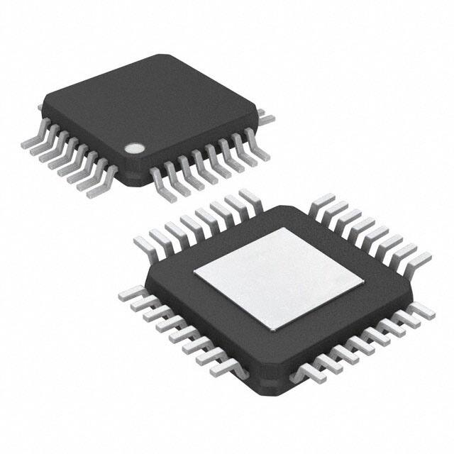


 工商网监
湘ICP备2023018690号
工商网监
湘ICP备2023018690号
